
The semiconductor industry faces a fundamental challenge: as process integration grows increasingly complex with 3D transistor architectures and multi-level interconnect stacks, many critical defects have become optically unresolvable. PDF Solutions’ DirectScan solution, powered by the eProbe e-beam inspection tool, addresses this challenge with a fundamentally different approach to voltage contrast inspection.
At the 2025 PDF Solutions Users Conference, we gave a presentation on eProbe’s technology, its applications, value proposition and industry adoption. The presentation can be found here.
What is The Inspection Gap in Advanced Nodes?
Modern semiconductor manufacturing has evolved dramatically. FinFETs have given way to gate-all-around (GAA) nanoribbon transistors, while middle-of-line (MOL) stacks have grown more intricate with multiple patterning colors. The result is that killer defects are increasingly buried within these 3D structures, rendering traditional optical inspection methods, the workhorse of the industry for decades, inadequate.
Moreover, defects in advanced nodes are rarely random. They emerge at specific process-layout combinations, often called hotspots, appearing systematically at particular locations within dies and wafers. Many yield issues are product-specific, driven by unique layout weaknesses inherent to each design.
This creates a paradox: we need e-beam voltage contrast inspection to detect electrically relevant defects, but e-beam inspection is inherently slower than optical methods. The solution lies in extreme efficiency.
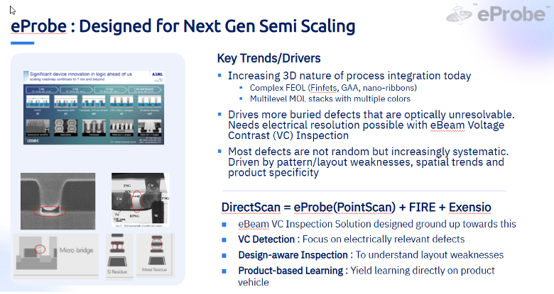
What is DirectScan? – A Paradigm Shift in E-Beam Inspection
DirectScan combines three key components: eProbe (the e-beam tool), FIRE (PDF’s GDS analysis platform), and Exensio (for data analysis). At its core is a technique called PointScan that fundamentally reimagines how e-beam inspection works.
Conventional e-beam inspectors operate by rastering across regions of interest, capturing complete images, then performing die-to-die comparisons to identify defective pixels. They scan everything, including dielectric areas that yield no useful voltage contrast signal, without knowledge of what features they are inspecting.
eProbe’s PointScan, by contrast, functions as a contactless electrical tester. It jumps from one device under test (DUT) to another, measuring voltage contrast at specific pads of interest while skipping dielectric regions entirely. The tool knows precisely what it’s scanning at each moment: the exact “GPS location” and layout attributes of every inspection point. This is design-aware inspection in its truest form.
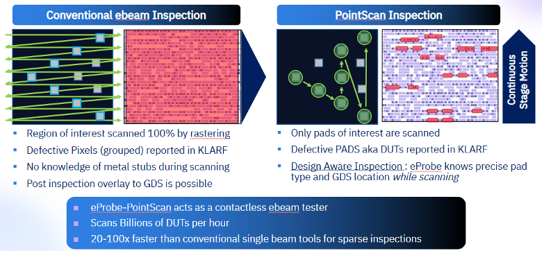
The efficiency gains are substantial. In one back-end-of-line example targeting vias opened at metal-3, FIRE analysis identified that only 3 meters of the 120-meter total metal runner length required inspection: just 2.5% of the available area. For MOL gate-drain short detection, only 1% of total contacts needed scanning. Even in less dramatic cases like gate stringer inspection, where 30% of contacts require examination, the tool still avoids scanning 50-75% of the dielectric area, resulting in overall area inspection of less than 10% compared to conventional methods.
Depending on DUT density, PointScan can achieve throughput 20-100 times faster than conventional single-beam tools while scanning billions of DUTs per hour.
How to leverage Design-Aware Learning and Attribute Analysis in ebeam inspection?
DirectScan’s integration with FIRE enables sophisticated layout analysis across multiple layers. For each contact or pad, FIRE extracts relevant attributes: whether it’s a drain or gate contact, transistor threshold voltage, polarity, proximity to diffusion breaks, and more.
The eProbe KLARF output includes an attribute ID that maps to these pre-mined characteristics. This enables direct calculation of fail rates for any attribute or combination, quickly revealing which transistor types or layout configurations are most susceptible to defects. This actionable information allows process engineers to refine subsequent inspection recipes, focusing progressively on the most critical failure modes.
This capability transforms inspection from simple defect detection into a rapid learning vehicle for understanding product-specific weaknesses.
What are the Emerging Applications of DirectScan?
PointScan’s reduced charge deposition offers critical advantages for challenging inspection scenarios. Backside power delivery network (BSPDN) wafers and 3D DRAM present unique difficulties because bonded wafers create insulating layers that prevent charge from reaching the grounded backside. This charge accumulation causes beam deflection and defocus, making conventional e-beam inspection problematic.
PointScan’s dramatically lower charge-per-area deposition alleviates these issues, making previously intractable inspections feasible. PDF has successfully demonstrated applications on both BSPDN and 3D DRAM wafers.
Perhaps most innovative is the controlled “charge and sense” capability, which is only possible with PointScan. The tool can dwell at specific locations to deliberately charge them, then jump to other locations to collect voltage contrast signals. This has proven particularly valuable for detecting shorts in DRAM arrays. By charging wordline contacts, specific island nodes turn bright, revealing shorts to floating neighboring contacts, an inspection methodology impossible with raster scanning.
What are Examples of Industry Adoption and Applications of DirectScan?
Since early 2022, eProbe systems have been deployed at leading-edge logic fabs, with two tools currently in high-volume manufacturing and a third ramping. Applications span the process flow:
Leading-Edge Logic:
- MOL: GAA gate-drain shorts, gate-contact opens, gate-epi/silicide opens
- BEOL: Systematic contact opens and metal shorts at M0, 1x, and 2x layers
- BSPDN: Contact opens and shorts in power vias and source/drain vias
- Leakage estimation in random logic
Leading-Edge DRAM (2024-2025):
- Periphery inspection: Gate-gate stringer shorts, gate-drain shorts, wordline-wordline shorts and opens with localization
- Array inspection: Storage node shorts using controlled charge and sense
The solution delivers high-throughput product inspection with faster turnaround time for identifying process weaknesses, reduced wafer charging for advanced bonded structures, and enables entirely new inspection methodologies through controlled charge and sense.
결론
As semiconductor scaling pushes into increasingly complex 3D architectures, inspection must evolve beyond traditional paradigms. DirectScan represents this evolution—combining targeted PointScan efficiency, design-aware intelligence, and product-specific learning to address the inspection challenges of next-generation devices. For an industry where buried, systematic, and electrically relevant defects dominate yield loss, this approach offers a path forward that balances the sensitivity of e-beam inspection with the throughput demands of volume manufacturing.