
What is the Data Challenge in Semiconductor Manufacturing?
The semiconductor manufacturing industry faces an unprecedented data challenge. Modern fabrication facilities now grapple with test programs containing over a million test items, generating gigabytes of data per chip across probe, assembly, and test operations. The largest deployments have reached the multi-petabyte range, creating a fundamental problem: traditional business intelligence tools simply cannot handle semiconductor-scale data with millions of columns and rows.
Mike Campbell, Qualcomm’s Chief Supply Chain Officer, recently said that as a result of the increased complexity of advanced packaging, the amount of manufacturing and test data that semiconductor companies need to analyze has increased sixfold since 2022. At the same conference, Aziz Safa, Intel Corporate VP and GM Intel Foundry Automation, noted: “We have 600 petabytes of data across Intel. The challenge that we have is to be able to run algorithms on the areas where we need that data to solve problems.”
Comments from John Kibarian, PDF Solutions’ CEO, mirrored those remarks made during the PDF Solutions Users Conference in December. In many cases, he said, no more than 5% of the collected semiconductor manufacturing data is used in analytics. Yet more than ever, access to timely analytics is critical to quickly ramp the yield of new advanced process nodes or ensure the quality of complex packages. In this context, it is critical to find new innovative ways to scale the ability to analyze semiconductor data.
PDF Solutions has developed a comprehensive strategy to enhance the capability of its Exensio data platform, already widely used across the semiconductor industry to address this challenge by combining scalable analytics infrastructure with advanced AI capabilities including Large Language Models (LLMs) and autonomous agents.
This approach represents a fundamental rethinking of how semiconductor manufacturers can extract actionable insights from massive, complex datasets.
Can Business Intelligence Solutions Handle the Very Large Amount of Data Produced in Semiconductor Manufacturing?
Traditional business intelligence (BI) tools face critical limitations in semiconductor manufacturing environments. They rely on local memory, which severely restricts analysis and machine learning capabilities. They lack computational and organizational scalability often related to the specific characteristics of semiconductor data that may have hundreds of thousands or even millions of parameters to analyze. Think of a table with a million columns and hundreds of thousands of rows. Visualizing this type of dataset in a traditional data analytics or BI tool has reached its limit, and this approach will not address the future needs of an industry where data size and complexity keep increasing.
Typically, engineers develop bespoke scripts based on summary statistics disconnected from the original data sources, and these scripts are typically served without the infrastructure for robust sharing across the organization.
Scalable Analytics – An Innovative Solution Architecture to Deliver High Scalability in Handling Semiconductor Manufacturing Data
PDF Solutions’ answer is a new parallel and distributed data architecture with dynamic partitioning. Rather than bringing raw data to the client for analysis, the system keeps data in the server layer and delivers only the visualizations needed by users. This thin-client approach enables the system to scale dynamically based on current needs by caching in the data layer for faster access and pre-configured analytics running continuously across all available data.
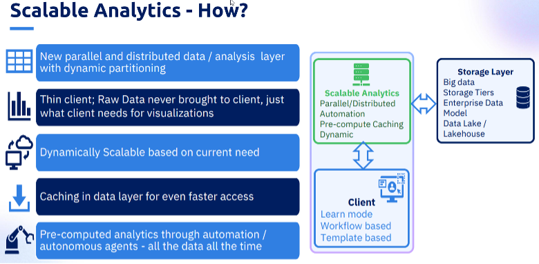
The results are striking. Benchmark testing shows approximately 25-fold performance improvements on typical large test programs with the ability to work with one million test items and beyond, a scale of analysis previously impossible. The system achieves this through parallelizable performance across both rows (individual die) and columns (test parameters), combining static compute nodes with burst cloud computing for cost-effective scaling to extremely large datasets.
Enterprise ModelOps at Scale – How to Manage AI Model Lifecycle at Scale Across the Semiconductor Industry?
PDF Solutions recognizes that deploying AI in semiconductor manufacturing requires more than just training models; it demands a complete operational infrastructure. Its strategy addresses three major operational challenges: deployment bottlenecks caused by manual handoffs and brittle integrations, data friction from building custom pipelines instead of leveraging existing systems, and governance risks from poor lineage between production models and training parameters.
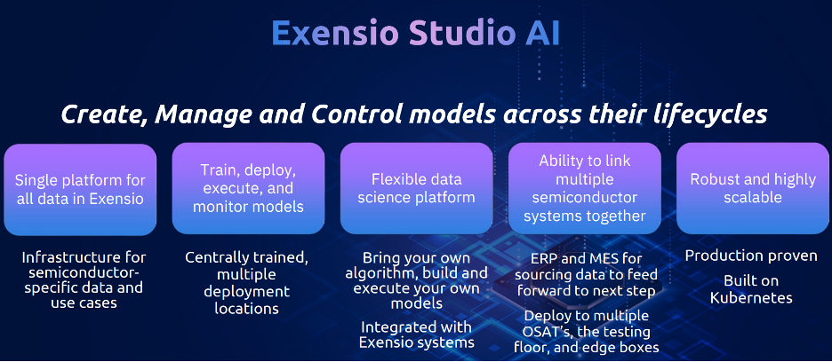
The company announced Exensio Studio AI, which integrates capabilities from Tiber AI Studio, a solution formerly owned by Intel, built to empower data scientists from code to production, with Exensio ModelOps built for semiconductor data and focused on deploying models at the edge. The roadmap for Exensio StudioAI includes several key capabilities rolling out through 2026, including the ability for engineers to bring their own models. An enterprise-grade model registry will enable model lifecycle governance, tracking and sharing, with full data traceability ensuring that any model’s training inputs are always known.
Semiconductor Semantic Data model – How to Break Down Data Silos Across the Various Data Sources and Repositories?
One of the most significant challenges in semiconductor manufacturing is the fragmentation of critical data across isolated systems. Yield data sits in one place, design diagnosis information in another, and equipment telemetry in yet another. This fragmentation blocks the correlation of volume yield data with physical layout features and prevents engineers from connecting specific process excursions with final yield outcomes.
PDF Solutions addresses this through aggressive data integration efforts. Its platform is extending beyond traditional manufacturing analytics to create more complete end-to-end data models that are highly customizable and extendable. For example, integration with Siemens Tessent provides a single interface for yield-design correlation, while equipment data integration combines equipment health and usage information with yield data to enable LLM-driven overall equipment effectiveness improvements and root cause analysis of excursions.
Central to this effort is the development of a semiconductor-specific semantic data layer that maps the complex relationships between yield, design, process and tool data. This allows alignment and a link data across domains and sources in the Exensio data platform. It also allows LLMs to interpret disparate data types as a unified whole rather than struggling with disconnected information sources.
Workflows as the Foundation – How to Orchestrate Analytics Operations to Deliver Reliable AI Solutions in Semiconductor Manufacturing?
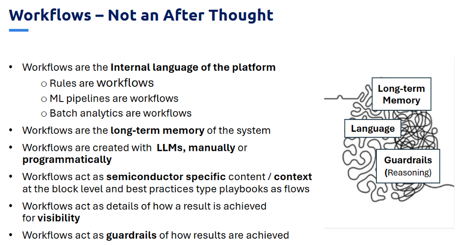
A key architectural decision in PDF Solutions’ platform is to treat workflows as the internal language of the system. Every analytic operation, whether rules, machine learning pipelines, or batch analytics, is expressed as a workflow. This provides several critical benefits.
Workflows serve as the long-term memory of the system, capturing not just results, but the complete methodology used to achieve them. They can be created from learn mode, through LLMs, manually, or programmatically, and can be embedded within larger workflows for maximum reusability. Engineers may never need to directly interact with a workflow, but the capability is there when needed.
Critically, workflows act as semiconductor-specific content and context, encoding best practices as reusable playbooks. They provide transparency into how results are achieved and serve as guardrails for AI reasoning, helping prevent the hallucinations that can occur when LLMs operate without domain constraints.
How to Ingrate LLM and Agentic AI in the Overall Semiconductor Manufacturing Analytics Platform?
PDF Solutions’ ultimate goal is to enable engineers to interact with manufacturing data at a higher level of abstraction. Rather than requiring deep technical knowledge of query languages and data structures, it envisions a system where engineers can ask natural language questions and receive actionable insights.
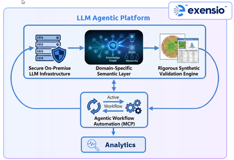
Achieving this vision requires what it calls a “Semantic, Agentic, and Secure” infrastructure. The semantic layer is built on 30 years of domain expertise, creating semiconductor-native knowledge graphs that encode the fundamental data hierarchy of manufacturing. This anchors LLM reasoning in the structural reality of manufacturing data, eliminating ambiguity and providing the ground truth context needed to prevent hallucinations.

For example, the system understands that CV refers to Characterization Vehicle, that yield represents the results of die binning, and that the data hierarchy flows from lot to wafer to die to package. It knows that common analytical tasks include yield trending, bin Pareto analysis, and univariate screening. This enables engineers to ask questions like “Show me the yield trend over the last week” or “What is the root cause of low yield in lot XX?” and receive meaningful, accurate responses.
The platform integrates the Model Context Protocol, transforming Exensio into a truly agentic system. Rather than just summarizing text or answering questions, the system can autonomously plan and execute complete workflows from raw data ingestion through complex plot generation.
To ensure reliability and transparency, any agentic tasks are executed using scalable analytics workflows. They can be viewed, saved and modified by engineers at any time to ensure total transparency into the LLMs actions.
Recognizing the extreme sensitivity of semiconductor manufacturing data, PDF Solutions offers a fully air-gapped, on-premises LLM infrastructure option designed for intellectual property sovereignty. This ensures that sensitive yield data and proprietary models never leave secure firewalls, eliminating reliance on third-party cloud providers.
The Path Forward
PDF Solutions has invested 18 months in research and development on technology selection, validation, and tuning, engaging a large group of architects, developers, quality assurance specialists, designers, and product managers now working on the platform. Scalable analytics will be available to early adopters in early 2026, with broader availability to Exensio Cloud customers starting in late 2026.
The company’s vision addresses what they identify as the critical industry challenge: de-risking AI adoption by securely scaling execution and maximizing return on investment from legacy data, while simultaneously future-proofing infrastructure for the rapidly emerging age of LLMs and autonomous agents.
By combining massive-scale data processing, enterprise ModelOps, intelligent data integration, and agentic LLM capabilities, all grounded in deep semiconductor domain expertise, PDF Solutions is working to transform how the industry extracts value from the exponentially growing volumes of manufacturing data. Its approach suggests a future where engineers spend less time wrestling with data infrastructure and more time solving the complex yield and quality challenges that define success in semiconductor manufacturing.
You can access all the content of the 2025 PDF Solutions Users Conference at this link.