Detect the Undetectable

Semiconductor 3D structures can include buried defects that are difficult to detect, resulting in low-level leakages and variations that can lead to significant variability in interconnect resistance and transistor performance, leading to months of extra design cycle time.
But with PDF Solutions’ Design-for-Inspection™ you can find these problems during “Middle of Line” inline inspection and accelerate your time to market by up to 4 to 6 months.
DOWNLOAD the DFI datasheet
What is “Design-for-Inspection”?
Our Design-for-Inspection System, or DFI™ System, is a contactless e-beam measurement system that can detect electrically relevant defects buried inside of 3D structures at a rate of hundreds of millions of DUTs per hour. Fast enough to be used inline during middle of line semiconductor manufacturing.

Early Visibility into Potential Reliability Risks
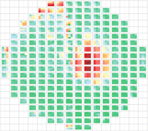
The DFI System efficiently scans billions of structures per wafer to identify tiny leakages at PPM to PPB levels and provide unique reliability insights into latent weak spots in a die. The system provides a high resolution map of every die for single fail types or a composite map for all fail types. This detailed across-die measurement provides foresight and enables better risk screening per die than gross methods such as GDBN (Good Die Bad Neighborhood)
Production-Proven
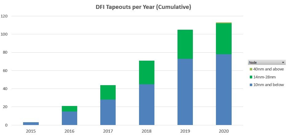
Our DFI System has been realized in over 120 tape outs to date, spanning 7 advanced process nodes from 28nm down to 5nm. In addition, over 60 PDF Characterization Vehicles have been taped out with DFI content.

How does the DFI System Work?
The DFI System is a combination of patented IP cells that are inserted into a design, and specialized, high-performance e-beam hardware that read the electrical response of those IP cells. Together, they can help identify process and layout sensitivities that limit yield, performance, and reliability to provide foresight into design issues that normally cannot be seen or measured until months later and result in costly design respins and delayed time-to-market.

High Performance, Inline E-Beam Inspection
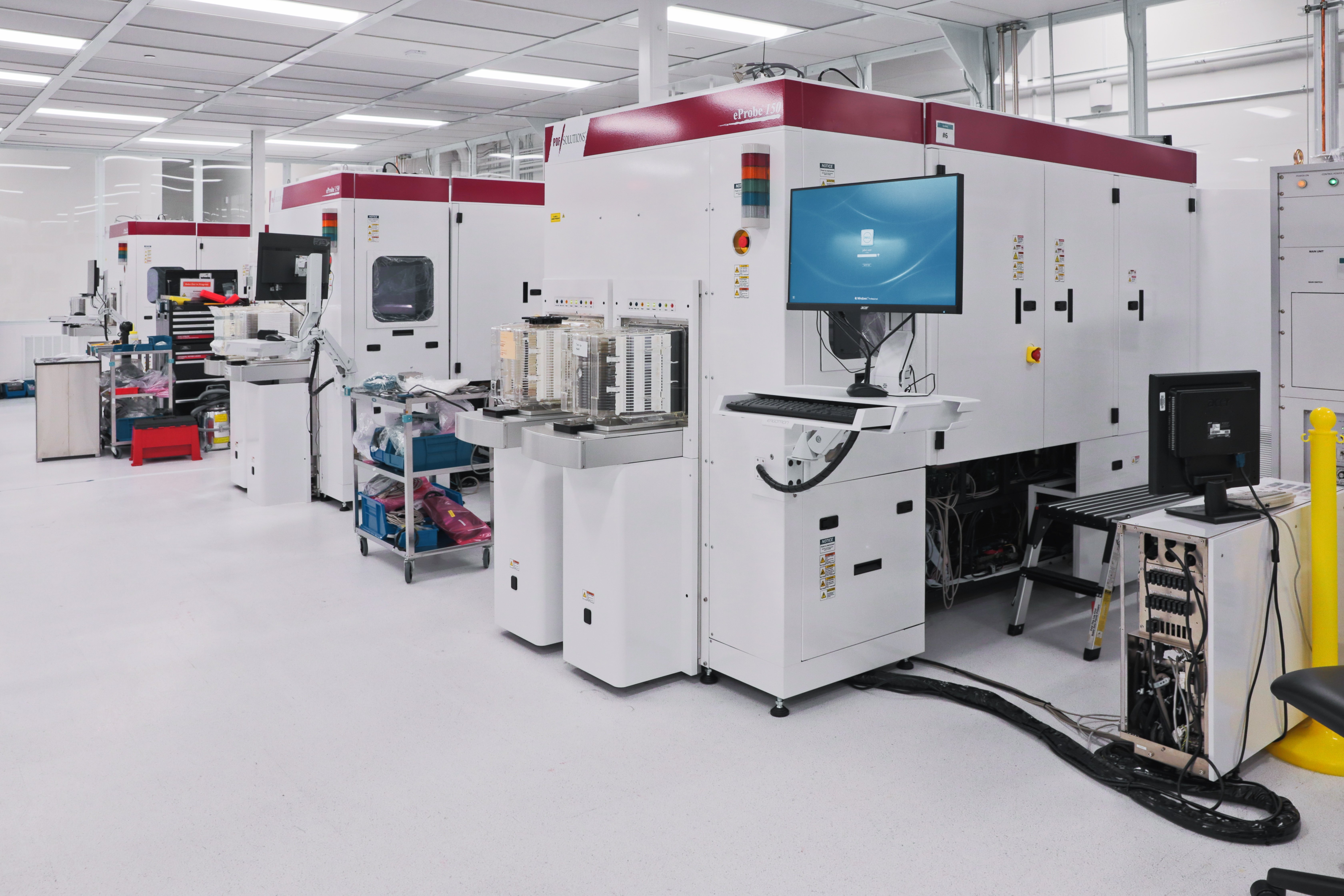
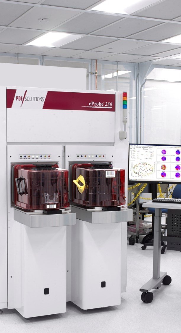
Our patented IP cells are read in middle-of-line manufacturing by our contactless e-beam test measurement systems, the eProbe® 150 and 250. These systems are currently deployed at multiple sites worldwide and are in active use for yield learning at multiple nodes (22nm, 14nm, 7nm and 5nm). Throughput performance on the eProbe 250 is well in excess of 100 million DUTs per hour, fast enough for inline inspection.
