
 The compound semiconductor industry faces a persistent challenge: defects introduced during crystal growth and epitaxy often don’t manifest until final test or assembly, when it’s too late and too expensive to prevent yield loss. For manufacturers working with silicon carbide (SiC), gallium nitride (GaN), and gallium arsenide (GaAs) materials, the question isn’t whether substrate defects will impact yield, but how to predict and mitigate that impact before wafers move downstream.
The Compound Semiconductor Manufacturing Challenge
Compound semiconductors have become indispensable for applications silicon cannot address. Their high electron mobility enables the 5G/6G RF chips and high-speed electronics that power modern communications. Their direct bandgap properties make efficient light generation possible in LEDs, laser diodes, and infrared sensors. Their high breakdown voltage, combined with excellent thermal conductivity, allows operation under the extreme conditions required for EV power electronics, fast chargers, and renewable energy systems.
However, these performance advantages come with manufacturing complexity that creates three critical problems:
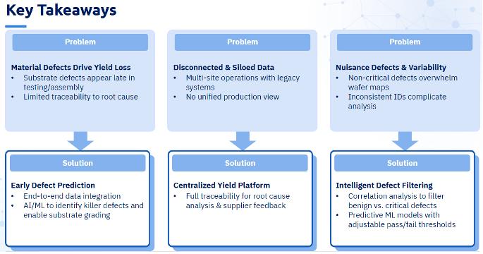
Material defects at the source. Crystal growth and epitaxy are expensive processes where defects originate, but these defects often only become apparent much later during testing and assembly. By that point, significant value has been added to wafers that will ultimately be scrapped or yield poorly. Tracing these failures back to their origin in the substrate or epitaxial layers is difficult without integrated data systems.
Siloed data across disparate systems. Manufacturing data lives fragmented across multiple sites, fabs, and equipment systems. Without a centralized view linking substrate defects, inline process data, and final electrical test results, root cause analysis becomes a time-consuming manual exercise rather than a systematic engineering process.
Nuisance defects overwhelming the signal. Wafer defect maps get flooded with non-critical “nuisance defects” that don’t impact yield, masking the truly killer defects that matter. Add in data quality issues like substrate ID changes from rework and lot splits, and the noise-to-signal ratio becomes problematic for meaningful analysis.
An End-to-End Data Integration Approach
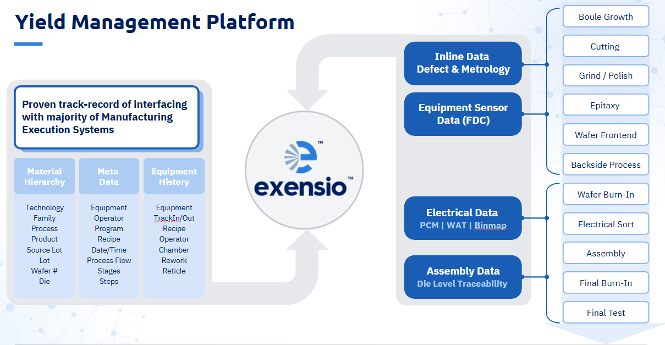
Addressing these challenges requires a platform that can unify data across the entire manufacturing flow—from boule growth through epitaxy, wafer frontend processing, and ultimately to assembly and final test. The Exensio platform integrates inline defect and metrology data, equipment sensor data, electrical test results, and assembly traceability into a single coherent hierarchy.
This unified data structure enables tracing a failing die all the way back to the raw material lot, the specific tool and recipe used, and even the process conditions that produced it. For compound semiconductor manufacturers, this complete traceability is the foundation that makes predictive machine learning practical.
The platform is currently deployed at over 100 semiconductor companies worldwide, with more than 10 compound semiconductor manufacturers using it for enterprise-wide yield management across IDMs, foundries, and fabless operations.
Machine Learning Method: From Substrate Defects to Yield Prediction
The core innovation is connecting substrate defects, those that occur at the very beginning of the manufacturing flow, with final pass/fail outcomes at electrical test. This enables identifying which defect types truly impact yield, predicting yield earlier in the process, and even grading substrates before they move downstream.
The Analytics Flow
The machine learning workflow consists of five key steps:
- Data Collection and Mapping. Substrate defect data (or inline defect data from later process steps) is collected along with electrical test binmap data. A Python script maps absolute defect coordinates to the die coordinate system defined by the binmap configuration, enabling direct die-by-die comparison of defect counts with electrical test results.
- Intelligent Defect Filtering. Not all defects are created equal. The Python script identifies and filters two special categories:
- Strong killers: Defects with a kill ratio greater than 0.9 that almost always cause die failure. Dies containing strong killers are automatically marked as fail.
- Negatively correlated defects: Defects that oddly appear more frequently in passing dies than failing ones, indicating they’re not yield-limiting.
Both categories are removed from the training dataset so the model focuses only on meaningful predictive signals.
- Feature Reduction. Defect features are standardized, and Principal Component Analysis (PCA) is applied, retaining 95% of the variance. This dimensionality reduction captures the important information while preventing the model from being overloaded with redundant or less useful features.
- Model Training. An XGBoost classifier is trained on the filtered, reduced feature set using 10-fold cross-validation with balanced classes to prevent bias toward a single outcome. The model learns to predict die-level pass/fail probability based on defect characteristics.
- Prediction and Evaluation. The trained model predicts whether each die will pass or fail electrical test. An override rule ensures that any die with strong killer defects is automatically set to fail regardless of the model’s probability output. Results include a confusion matrix, classification metrics (precision, recall, F1 score), and most critically, predicted vs. actual wafer yield comparisons.
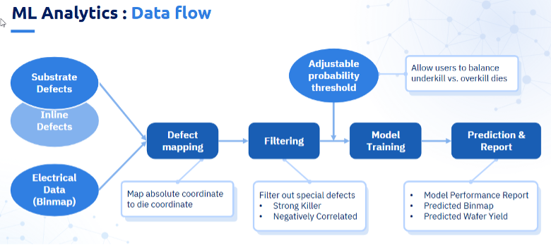
Balancing Underkill vs. Overkill
A key feature is the adjustable probability threshold that allows users to tune the model’s behavior based on business priorities. A lower threshold increases underkill risk (letting bad dies slip through) but may decrease overkill (scrapping good dies). A higher threshold does the opposite. This flexibility lets engineers balance yield loss against manufacturing costs based on their specific economic constraints.
Interactive User Interface for Production Use
Analytics are only valuable if engineers can actually use them in their daily work. The implementation includes an interactive user interface designed for intuitive navigation:
- A landing page provides an overview and sidebar navigation
- An introduction page lists input requirements and data import procedures
- A usage page guides users through input settings and shows how to replace the default model with customized Python scripts
- The prediction page is where the real work happens, with input fields for selecting grouping columns, running defect coordinate mapping, setting pass/fail thresholds, and executing predictions
- Results sections display special defect categories, classification performance metrics, three-way wafer map comparisons (actual, predicted, and difference maps showing false negatives and false positives), and tables/scatter plots of actual vs. predicted yield by wafer and lot
- An appendix page collects background knowledge supporting the template
Critically, users can open and modify the Python script directly within the template, allowing them to adapt the model to their own process knowledge and requirements.
Real-World Application: Silicon Carbide Case Study
The approach has been validated with silicon carbide, a wide bandgap material critical for EV and high-power applications. In this case study, substrate defects were mapped to electrical test results, defects were filtered and classified, and the XGBoost model was trained to predict die-level yield.
The results demonstrate several practical capabilities:
- Early yield prediction based on substrate defects before significant value-add
- Identification of killer defect types that truly impact yield vs. benign nuisance defects
- Substrate grading potential before wafers enter expensive downstream processes
- Visual evidence through binmap comparisons that engineers can use to guide decisions
- Quantitative metrics for model performance and yield prediction accuracy
Solving the Core Manufacturing Challenges
This integrated approach directly addresses the three fundamental challenges in compound semiconductor manufacturing:
Material defects appearing late: By using end-to-end data integration and machine learning, manufacturers can predict defect impact much earlier in the flow, identify killer defects, and enable substrate grading before wafers move downstream.
Disconnected siloed data: The platform unifies data from multiple sites and legacy systems into a single environment, providing complete traceability for root cause analysis and more effective supplier feedback.
Nuisance defects and variability: Intelligent defect filtering and correlation analysis separate benign defects from those that truly matter, while predictive ML models with adjustable thresholds let users balance underkill and overkill based on their specific risk and cost priorities.
The Path Forward
As compound semiconductors become increasingly critical for next-generation applications, from 5G/6G communications to electric vehicles to renewable energy, manufacturers need tools that can keep pace with the complexity. The combination of unified data integration, intelligent filtering, and machine learning prediction provides a path to earlier intervention, smarter decisions, and ultimately higher yields.
Exensio platform is proven with over 10 compound semiconductor manufacturers already using it in production. As the industry continues to scale, the ability to predict and prevent yield loss from source defects will become not just an advantage, but a requirement for competitive manufacturing.