
Leading-edge innovation is moving into the package and it’s changing what the industry needs to measure, how data has to flow, and who needs to collaborate. Here’s what that means for characterization and test, adapted from Ramune Nagisetty’s presentation at IMAPS CHIPcon 2026.
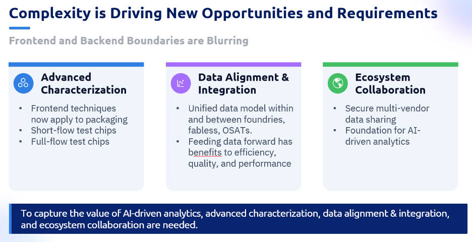
For decades, semiconductor progress was a story about the transistor: smaller, faster, cheaper. That era hasn’t ended, but it now shares the stage. Leading-edge innovation is increasingly driven by advanced packaging, and the once-clean line between the front end (silicon) and the back end (packaging) is dissolving. Below, we walk through what’s driving the shift and the three capabilities the industry needs to turn packaging complexity into an advantage.
Why has advanced packaging become the main driver of leading-edge innovation?
Moore’s Law has evolved along a third vector. The original Moore’s Law was an economic observation, cost per transistor halving roughly every two years. Dennard scaling (the dimensional shrink) stalled in the early 2000s, but performance kept improving along two additional paths: material and device innovation (strained silicon, high-k metal gate, FinFET, gate-all-around) and design-technology co-optimization (DTCO) (from diffusion breaks and contact overactive gate to backside power delivery).
The third vector is advanced packaging and heterogeneous integration, which enables system-technology co-optimization (STCO). As we like to put it: if silicon is the king on the chessboard, advanced packaging is the queen; versatile, powerful, and strategic.
How big is this shift, really?
Big enough to reshape roadmaps. The 2.5D and 3D packaging market is projected to grow at roughly a 26% CAGR, reaching about $80B by 2033 according to a recent report by Bloomberg Intelligence, with hybrid bonding becoming the preferred solution for cloud AI and autonomous applications, and AI package sizes are on track to grow several-fold as designs add compute and memory.
The leading edge already shows this trend: flagship AI products integrate multiple reticle-limited die on large silicon interposers with stacked high-bandwidth memory. Interposer roadmaps point toward 14 reticles and beyond. Advanced packaging has become an essential lever for performance gains.
What does advanced packaging change about characterization?
Advanced packaging has yield sensitivities and defect mechanisms, buried voids, overlay/misalignment errors, mechanical stress transferred into active silicon, we are now applying proven test-chip characterization that has typically been used on silicon to packaging features like RDL, micro-bumps, TSVs, and hybrid-bond interfaces. With 800+ Characterization Vehicle (CV®) designs taped out on silicon, PDF Solutions applies the same methods to two types of test chip:
- Short-flow test chips — built for speed and sensitivity. A hybrid-bonding CV can test on the order of 10⁸–10⁹ pads for ~0.5-5 ppb observability, with excellent spatial resolution to the wafer edge. Sweeping DOEs across pad shape, size, pitch, and density, they detect buried voids and soft/hard opens, characterize overlay and process window sensitivity, and localize defects for failure analysis — at low cost and with fast turnaround.
- Full-flow test chips — add active transistors and circuits and greater resolution to quantify mechanical and stress effects on devices and interconnect, process-integration effects (CMP dishing/erosion, thermal expansion), and electrical integrity (TSV-to-silicon leakage, capacitance, resistance, opens). An embedded stress monitor can be read before and after die thinning, singulation, and packaging, at wafer sort, final test, and burn-in — and can be tested via JTAG or other interfaces. PDF has published results at ECTC that show thinner substrates have the highest stress, which relaxes at higher test temperatures.
If measurement is solved, why is chiplet data still so hard to use?
Because a chiplet product runs through a disaggregated supply chain. Wafers come from multiple foundries at different nodes; dies are combined via die-to-die, die-to-wafer, and wafer-to-wafer assembly; panels are singulated and surface-mounted; everything converges at assembly and test. Every hop is a facility with its own data mart and a material handoff, which leaves data scattered, siloed, and hard to trace at the unit level. Bluntly: the data is not AI-ready.
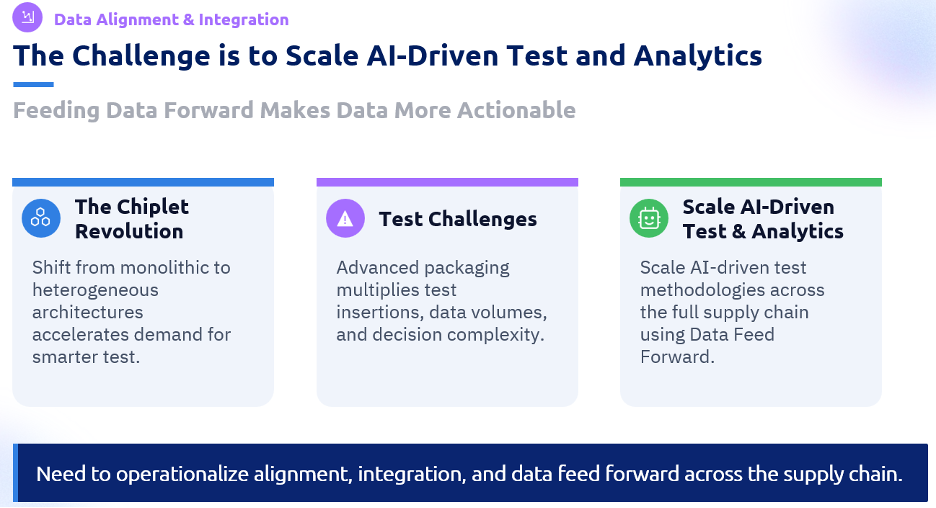
Chiplets also change the test paradigm three ways at once: more die and interfaces (more failure modes and coverage needs), more insertions and data (fab, wafer sort, assembly, package test, final test, burn-in, SLT), and interdependent decisions (results at one step shape the next, so errors compound). Conventional step-by-step testing ignores upstream intelligence leaving yield, quality, and performance on the table.
What is Data Feed Forward, and why does it matter?
Data Feed Forward (DFF) is the answer to a basic question: how do you get the right data to the right place at the right time across a distributed supply chain? DFF is operational, not a storage concept, the point is to make early data useful in real-time production decisions, turning upstream results into downstream process intelligence. It runs as a closed loop across five layers:
- Collect — ingest wafer sort, probe, and early-insertion data (parametrics, binning, wafer maps, context).
- Transform — convert raw data into predictions via feature engineering, rules, and model inference.
- Transport — deliver outputs securely across sites and partners through APIs and pipelines.
- Apply — feed results downstream to bin, skip, adjust, or flag.
- Write back — record outcomes for traceability and continuous model improvement.
Each layer adds value to, and leverages, the data before it, which is what makes AI-driven test scalable rather than trapped at a single insertion.
What’s the payoff of connecting the data?
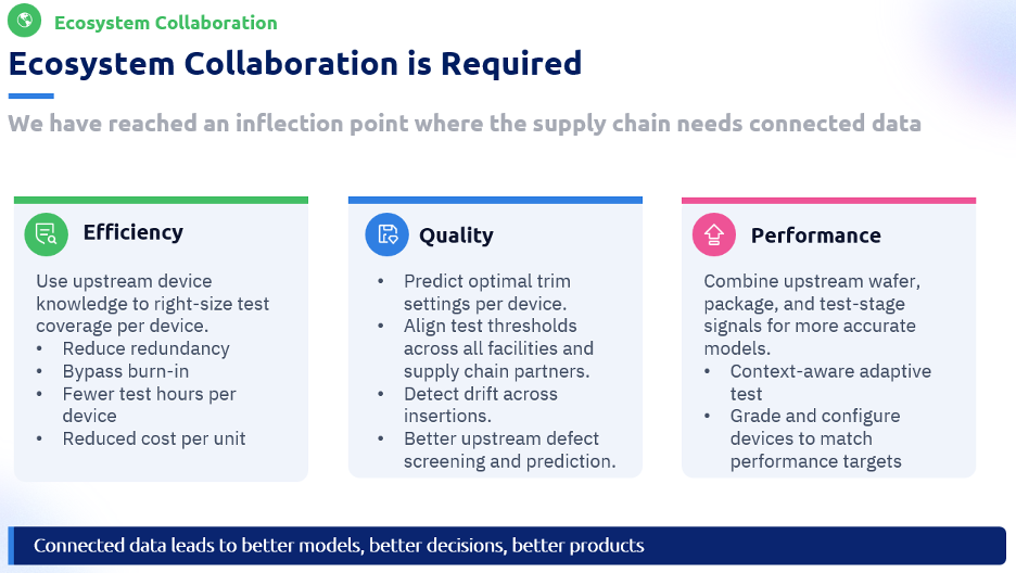
Connected data leads to better models, better decisions, and better products, in three areas:
- Efficiency — right-size test coverage per device: reduce redundancy, narrow a Vmin search for no-risk test-time reduction, and selectively avoid burn-in for predicted-good units (freeing capacity for at-risk devices).
- Quality — predict trim targets to prevent mis-trims, align test thresholds across facilities and partners, and detect drift across insertions — shifting quality from reactive to predictive.
- Performance — enrich in-line AI models with upstream history for context-aware adaptive test, smarter grading and routing, and assembly decisions that ooptimize cost and performance. As one industry leader noted, advanced packages are too expensive to throw away — so careful characterization and grading matter more than ever.
How does PDF Solutions make this real?
Through infrastructure built for the semiconductor supply chain, not retrofitted from generic tools. The Exensio® platform harmonizes data end to end across fab, OSAT, and test (FDC, wafer sort, final test, assembly). In-line traceability and scalable analytics address the multi-insertion, feed-forward needs of advanced packaging, while Exensio StudioAI provides a ModelOps layer for adaptive test: instead of static binning rules, AI models trained on correlated die and process histories are continuously updated and deployed across the supply chain via a secure Data Exchange Network enabled by secureWISE the secure remote connectivity solution most widely used across the semiconductor industry. It’s a materially different proposition from legacy adaptive test, and it’s what multi-chiplet assemblies now demand.
What are the key takeaways?
- Leading-edge innovation is now driven by advanced packaging, and front-end/back-end boundaries are blurring — especially where 300 mm tool sets are used for package integration.
- Advanced test-chip characterization methods once reserved for silicon now apply to packaging, via short-flow and full-flow test vehicles.
- Data alignment and integration across silos are foundational to AI-ready datasets.
- Data feed forward — an old idea whose time has come — improves efficiency, quality, and performance when operationalized as a closed loop.
- Chiplet-based architectures require connected data and ecosystem collaboration to deliver on their promise.
The industry has reached an inflection point. The characterization exists, the data architecture is understood, and the analytics platforms are in place. What remains is establishing close collaboration — letting data follow the product across companies and geographies- to create AI-ready datasets and bring best-in-class AI capabilities to the world of packaging.
Want to go deeper? Talk to PDF Solutions about advanced-packaging characterization, Data Feed Forward, and the Exensio platform at www.pdf.com and here
References
- Bloomberg Intelligence, Advanced Semiconductor Packaging Market growth outlook (2.5D/3D market, ~26% CAGR, ~$80B by 2033).
- TSMC CoWoS® roadmap discussion of interposer scaling toward 14-reticle and beyond.
- S. Saxena et al., IEEE ECTC, 2022; A. Piadena et al., IEEE ECTC, 2024 (advanced-packaging mechanical stress monitor results).
- K. Larsen, Synopsys, 3DIC integration options and design space.