
The previous posts in this series focused on two questions: why stress-related Local Layout Effects matter in advanced CMOS, and how they can be measured and modeled in a controlled way. The natural next step is the most important one: what do the silicon data actually show? Once the measurement flow and the TCAD framework are in place, the key issue is no longer whether layout-dependent stress exists, but how strongly it changes device behavior, which geometries matter most, and why some devices are much more sensitive than others.
The answer is both technically interesting and highly practical. The strongest layout-dependent effects appear around structures that modify the local mechanical boundary conditions of the channel, especially Diffusion Breaks and Gate Cuts. These features can alter the stress distribution enough to produce measurable shifts in drain current and threshold voltage, even when the nominal transistor dimensions are unchanged. The effect is not symmetric across device types: p-type FinFETs are consistently more sensitive, while n-type devices show smaller and more complex responses. In the measured 7nm structures, p-type variations can exceed 10% and, in some modeled cases, approach ±12%, whereas n-type shifts are typically below 5%.
This post focuses on those results. It explains what was observed around the main LLE mechanisms, why PMOS and NMOS behave so differently, and what the combined measurement-and-modeling flow reveals about the stress physics behind the electrical shifts.
1. Why Is PMOS Much More Stress-Sensitive Than NMOS?
One of the clearest outcomes of the study is that p-type FinFETs are much more sensitive to local layout perturbations than n-type devices. This is visible directly in the electrical data and remains consistent across the main LLE categories investigated. Near certain layout features, p-type devices show drain-current changes on the order of 10% or more, while n-type devices usually exhibit noticeably smaller shifts. In the broader calibrated analysis, the p-type response reaches roughly ±12%, whereas the n-type response generally stays below 5%.
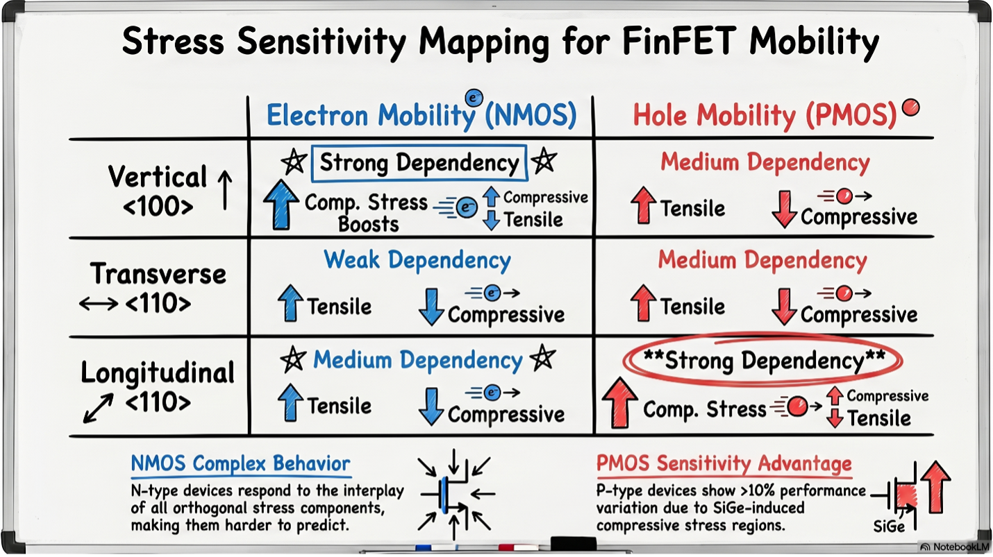
This asymmetry is one of the most important physical messages of the work. It shows that advanced-node layout sensitivity is not just about geometric proximity in a generic sense; it depends strongly on how different carriers respond to local stress. The electrical data make this immediately visible, but the stress analysis explains it more deeply: PMOS behavior is strongly driven by longitudinal stress variations, whereas NMOS is influenced by a more mixed combination of stress components, including vertical and transverse terms that can partially compensate one another.
That difference is exactly why some layout features that look modest from a geometric point of view can have a disproportionate impact on p-type devices. Once the local stress field is perturbed in the “right” direction, PMOS current can shift sharply. NMOS, by contrast, often responds more weakly and less monotonically because no single stress component dominates the response in the same way.
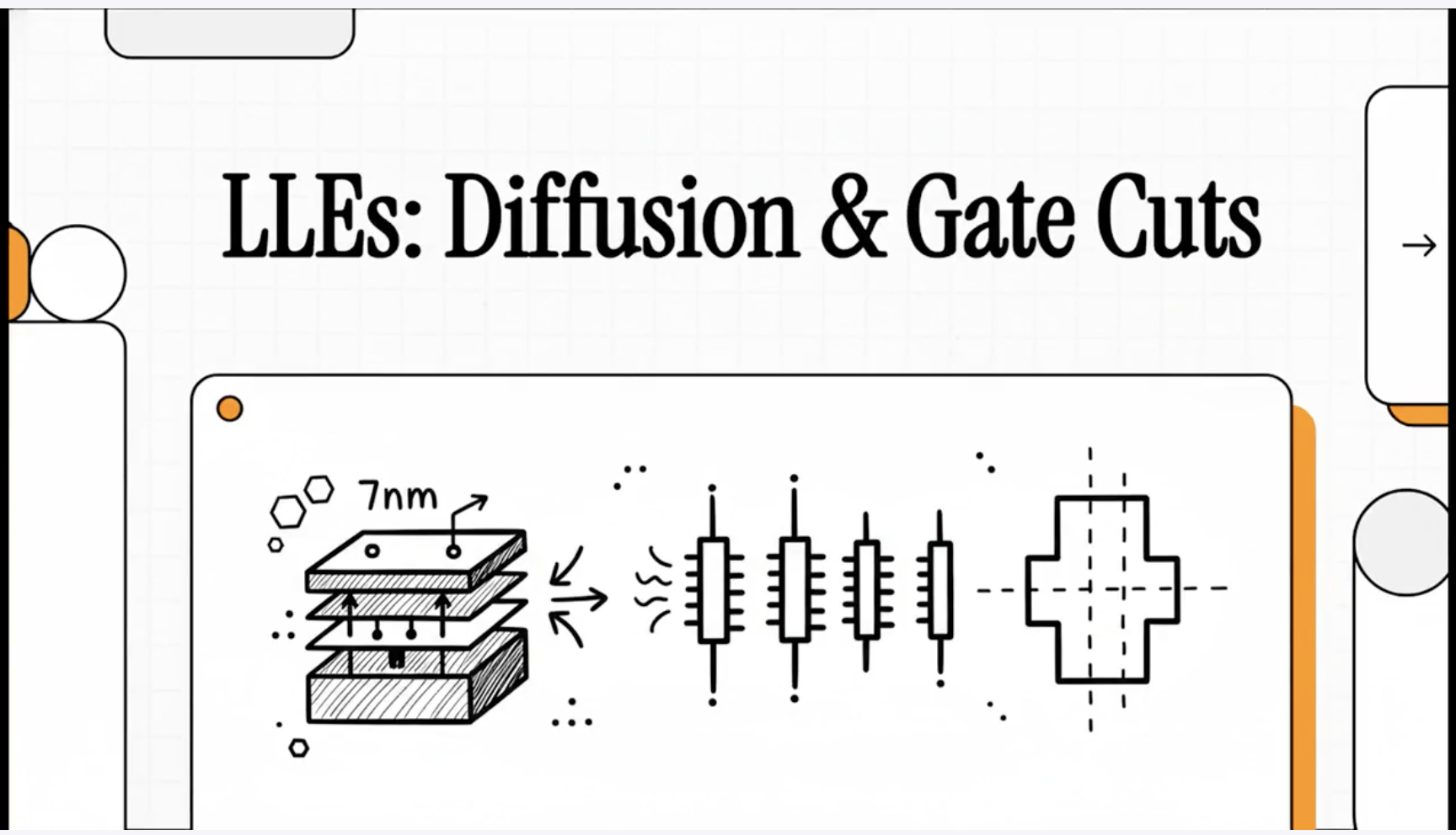
2. How Do Diffusion Breaks Lead to Large Consequences from Small Geometries?
Among the strongest LLE mechanisms observed in the study are those associated with Diffusion Breaks (DB). These structures provide local isolation between active regions, but they also change the mechanical environment seen by nearby transistors. In practice, the geometry and proximity of the diffusion break modify how stress develops and relaxes around the active region, and that altered stress field directly affects carrier transport in the channel.
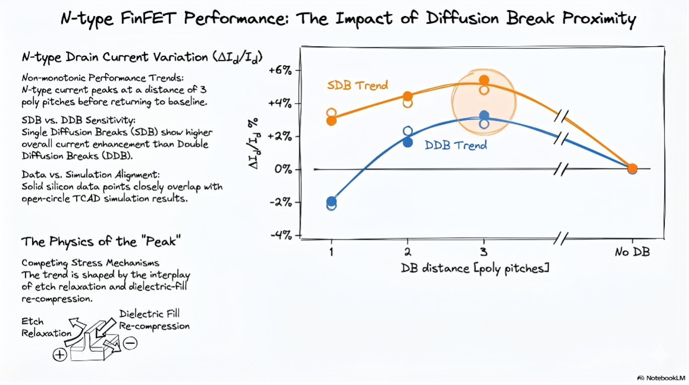
The measured data show that the electrical impact of diffusion-break proximity is especially strong in p-type devices. PMOS transistors near certain diffusion-break configurations exhibit a noticeable loss of drive current, with variations on the order of 10% in silicon and stronger trends reproduced in simulation depending on the exact layout condition. By contrast, NMOS transistors are affected more mildly, with smaller shifts and a less straightforward trend.
This is not simply a matter of physical distance. Diffusion breaks change the local stress boundary conditions in a way that interacts with source/drain stressors, isolation structures, and surrounding materials. For PMOS, where beneficial stress is more tightly linked to channel performance, disturbing that stress field can create a significant electrical penalty. That is why diffusion breaks emerge as one of the most important stress-related LLE sources in the entire study.
3. How Does Local Isolation Change the Stress State in Diffusion Breaks?
Although SDBs and DDBs both serve to electrically isolate transistors, their mechanical realization occurs at different stages of the fabrication process, creating profoundly different stress environments. DDB are defined early in the process, immediately after fin patterning, and thus before any engineered stress is introduced into the channel. In contrast, SDB, introduced to save approximately 30% of standard cell area, are typically etched late in the process, after the source and drain regions have been epitaxially grown and the stress is already “trapped” in the channel.
In PMOS devices, the SDB acts as a sudden release of mechanical energy. Because the cut occurs after the Silicon-Germanium (SiGe) epitaxial growth, the system loses the lateral structural support required to maintain the high longitudinal compressive stress. This mechanical “relaxation” is the primary cause of performance loss. Silicon data show that a PMOS device near an SDB can lose up to 15% of its linear drain current, whereas a DDB, being pre-formed, limits this degradation to approximately 8%.
TCAD analysis reveals even more complex physics for NMOS devices. Initially, the SDB trench etch causes a relaxation of the existing channel stress, shifting it toward a tensile state, which is beneficial for electron mobility. However, the subsequent process step involves filling the SDB trench with a dielectric isolation material. This dielectric fill exerts a new, opposing compressive force against the fin sidewalls. The final result is a delicate balance between the etch-induced relaxation and the dielectric-driven recompression. This interplay keeps NMOS current variations within a much narrower and less predictable window of -2% to +5% compared to PMOS.
These findings prove that, in sub-10nm nodes, the local shape of the active region and how it terminates in the layout are not merely geometric rules to prevent short circuits; they are actual mechanical engineering levers. Knowing that an SDB degrades PMOS performance much more severely than a DDB allows Design-Technology Co-Optimization (DTCO) teams to make informed decisions. They can strategically invest area in DDBs to preserve the speed of critical paths, while compressing area with SDBs where variability trade-offs are acceptable.
4. How Do Gate Cuts Turn the Metal Gate Into a Stress Source?
The second major LLE mechanism studied in depth is related to Gate Cuts (GC). At first glance, a gate cut might look like a layout-level termination detail. In advanced FinFET integration, however, it also changes the local mechanical boundary conditions associated with the gate stack.
In a Replacement Metal Gate flow, the work-function metal and the surrounding gate structure contribute directly to the local stress field, so changing the position or treatment of the gate cut can alter the stress state seen by the channel. The silicon data show that gate-cut proximity produces measurable and systematic shifts, again with a much stronger impact on p-type devices.
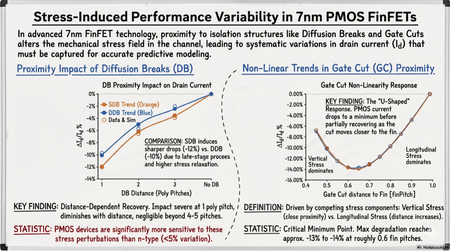
As with diffusion breaks, PMOS transistors near certain gate-cut conditions show clear current degradation or enhancement depending on the local stress redistribution, while NMOS responses remain smaller and more geometry-dependent. The calibrated 3D analysis reproduces these trends and confirms that the effect can be explained by changes in the local mechanical stress field rather than by a purely electrostatic interpretation alone.
This is a very important result for advanced-node design because gate cuts are common and unavoidable layout features. If they can measurably alter transistor stress, then they cannot be treated as neutral terminations. They become part of the variability problem and, eventually, part of the compact-model and DTCO problem as well.
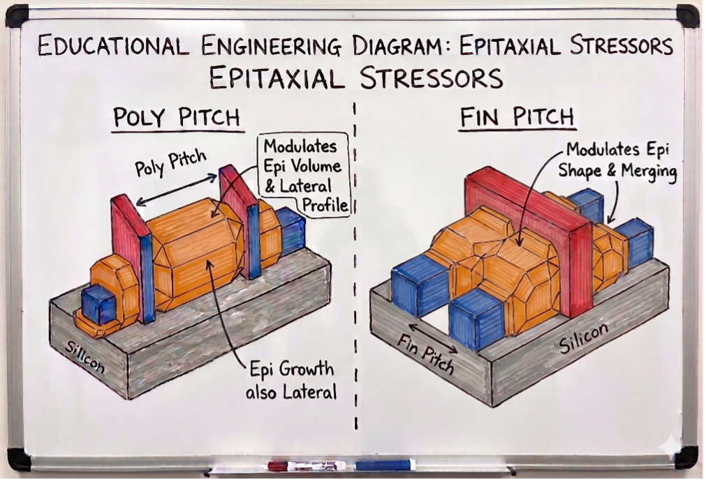
5. Poly Pitch and Fin Pitch: Smaller Trends, Still Meaningful
Beyond diffusion breaks and gate cuts, the study also examines layout-related effects associated with poly pitch and fin pitch. These mechanisms are often discussed in the context of scaling, routability, and density, but they also matter for device-level variability because they change the local neighborhood and therefore the way stress and other proximity effects are distributed around the transistor.
The measured and simulated results indicate that these pitch-related effects are real, but in many cases they are not as dominant as diffusion-break and gate-cut sensitivity. Their importance lies less in one dramatic shift and more in the way they modulate the local environment and interact with the stronger mechanisms. In other words, poly pitch and fin pitch are part of the broader stress context in which the transistor operates, even if they are not always the single strongest driver of variability by themselves.
That distinction is useful. It helps separate the primary stress modulators, such as DB and GC, from the more distributed geometric parameters that shape the background layout context. Both matter, but not in the same way. The strongest signatures in the data come from the local structures that most directly alter the channel’s stress boundary conditions.
6. What Is the Impact of Poly Pitch and Fin Pitch Variations?
The stronger PMOS sensitivity is not just a numerical observation. It has a clear physical explanation. The combined silicon-and-TCAD analysis shows that longitudinal stress is the dominant contributor to the p-type response. When local layout features such as diffusion breaks or gate cuts perturb this stress component, the effect on hole mobility can be large enough to create a substantial change in current.
That is why PMOS shifts are often both larger and more monotonic than NMOS shifts. Once the stress perturbation acts in the unfavorable direction, the electrical penalty appears clearly. In some conditions, this leads to current loss well above 10%. In other cases, the same stress sensitivity can be exploited beneficially, which is why strain engineering has historically been such an effective PMOS booster. The same physical lever that helps performance can also amplify layout-induced variability when local geometry is not controlled carefully.
This also explains why PMOS results are often the most visible part of the dataset. They are not simply “worse behaved.” They are more directly connected to the stress component that the layout perturbs most strongly. That makes them especially valuable as a stress monitor and especially dangerous if layout sensitivity is ignored.
7. Why Is the NMOS Response Smaller—and More Complex?
The n-type response is smaller, but not trivial. The data show that NMOS transistors are generally less sensitive to the same layout perturbations, yet their behavior is often less intuitive. This is because the relevant stress response is spread across multiple directional components rather than being dominated by a single one. Vertical and transversal stress terms can both contribute, and in some geometries they partially compete, reducing the net electrical shift or making the trend less monotonic.
That has an important modeling consequence. A simple “stronger/weaker stress” interpretation is often not enough for NMOS. To explain the measured response, the framework has to resolve the stress tensor and track how different components evolve with layout. That is why the 3D TCAD decomposition is so valuable: it reveals that the smaller NMOS sensitivity does not mean the effect is absent; it means the underlying physics is more distributed and therefore less obvious in the raw electrical data.
This is also one of the reasons why PMOS and NMOS cannot be treated with the same layout-sensitivity intuition. What helps explain one often does not directly explain the other. The asymmetry is not a side detail, it is one of the central design lessons of the work.
8. Why Is the Agreement Between Silicon Data and 3D TCAD So Critical?
One of the most convincing outcomes of the study is not only that the measured shifts are significant, but that the same trends are reproduced by the calibrated 3D TCAD framework. The agreement between silicon data and simulation is strong for both PMOS and NMOS, especially in the cases of Diffusion Break and Gate Cut sensitivity. That agreement matters because it shows that the observed effects are not arbitrary measurement artifacts or purely empirical anomalies, they are physically interpretable consequences of the local stress environment.
This agreement is particularly meaningful because some of the effects are relatively subtle, especially on the n-type side. Reproducing the sign, magnitude, and asymmetry of the results across multiple layout conditions is a much stronger validation than matching a single nominal curve. It shows that the combination of DOE, silicon measurement, and TCAD-based stress analysis is robust enough to explain what is happening at device level.
That is also what gives the later process studies their credibility. Once the framework is shown to explain the main LLE mechanisms on silicon, it becomes possible to use it to explore process knobs and integration changes with much more confidence. In that sense, the strongest result is not only the measured PMOS sensitivity, it is the fact that the same sensitivity becomes predictable.
9. What Do These Results Mean for DTCO and Layout Design?
The electrical shifts observed around diffusion breaks and gate cuts are not small curiosities. In advanced nodes, a 10% PMOS current penalty is not a minor modeling correction. It is large enough to affect timing, matching, design margins, and ultimately product behavior if not accounted for properly. That means these LLEs cannot remain hidden inside post-silicon debug or informal design intuition. They have to be represented in the way cells are developed, layouts are optimized, and compact models are built.
This is where the link to DTCO becomes especially important. Layout compaction techniques are meant to improve area and density, but the results here show that certain geometric choices can also amplify mechanical sensitivity. If diffusion breaks and gate terminations move closer to the active region, the transistor becomes more strongly coupled to its neighborhood. That creates a direct trade-off between area optimization and variability control.
In practical terms, this means LLE-aware design is no longer optional. The results support the need for layout-aware compact modeling, stress-aware PDK development, and design rules that reflect real mechanical sensitivity, especially for PMOS-critical paths and high-performance logic structures.
How Do These Data Change the Way We Think About Layout?
One of the most interesting consequences of these results is conceptual rather than numerical. Traditionally, layout is often treated as a geometric representation of a transistor that is already defined elsewhere by process and device physics. The results here point in a different direction: the layout is part of the physics. The local neighborhood around the device is not a passive backdrop. It contributes directly to the channel stress state and therefore to the electrical response.
Diffusion breaks and gate cuts make this especially clear because they are common, real, unavoidable layout features. They are not exotic process experiments. The fact that they produce measurable and predictable current shifts means that layout-sensitive variability is not an exception at advanced nodes, it is a structural property of the technology.
That idea is probably the most important design takeaway from the entire set of results. Once layout becomes a mechanical boundary condition, transistor variability can no longer be understood only from nominal width, length, and fin count. Local context must become part of both the physical interpretation and the design methodology.
Conclusion
The combined measurement-and-modeling analysis reveals a very clear picture. Diffusion Breaks and Gate Cuts are among the strongest stress-related Local Layout Effects in advanced 7nm FinFET structures, and their impact is especially severe for p-type devices, where current variations can exceed 10% and, in calibrated studies, reach roughly ±12%. NMOS devices are less sensitive overall, but their behavior is also more complex because multiple stress components contribute to the response.
These results matter for much more than device characterization. They show that layout-dependent stress is a real and predictable source of advanced-node variability, that the strongest effects can be isolated experimentally, and that the underlying physics can be captured with a calibrated 3D TCAD framework. That combination turns local layout sensitivity from an empirical annoyance into a problem that can be analyzed, modeled, and eventually engineered.
And once the main LLE mechanisms are understood, the next question becomes even more practical: which process knobs make these effects better or worse? That is where the discussion goes next.
What Comes Next
In the next article, we will move from the main layout-sensitive results to the process knobs that modulate them: Gate Cut timing, dielectric isolation materials, SDB trench width, spacer thickness, and temperature. Those studies reveal how strongly process integration can amplify or attenuate stress-related LLE behavior and why that matters for DTCO and process optimization.