
The previous post focused on the experimental side of the work: a high-density 7nm FinFET characterization chip, a structured DOE, and a measurement flow designed to isolate layout-dependent effects on silicon. But once those electrical results exist, an even more important question appears: how do you turn layout-dependent electrical shifts into a predictive physical model?
That is where TCAD becomes essential. Silicon measurements can show that one local geometry performs differently from another, but they do not directly reveal why. They do not show the underlying stress tensor, the process-induced strain distribution, or the relative contribution of longitudinal, vertical, and transverse stress components to the observed change in current or threshold voltage. To get that level of explanation, and ultimately prediction, a 3D TCAD framework was built and calibrated against electrical data from a commercial 7nm FinFET technology, with the explicit goal of modeling stress-related Local Layout Effects.
The result is not just a device simulator tuned to a nominal transistor. It is a process-aware, layout-aware, and experimentally calibrated framework designed to connect local geometry, process-induced stress, mobility perturbation, and electrical response. That combination is what makes the model useful not only for explanation, but also for DTCO, PDK development, and process optimization.
This post explains how that framework was built: what the model needed to achieve, how the calibration flow was organized, which physical effects were included, how stress was translated into electrical behavior, and why this type of modeling has become essential for advanced-node variability analysis.
1. Why Was a 3D TCAD Model Strictly Necessary?
A transistor affected by a nearby Diffusion Break or Gate Cut does not simply become “better” or “worse” in an abstract sense. Its behavior changes because the local process geometry perturbs the stress field, and that stress field modifies carrier transport through the anisotropic mechanical response of silicon. If the objective is to move from electrical observation to physical explanation, then the model has to connect layout geometry → process-induced stress → mobility perturbation → electrical characteristics. That is exactly the purpose of the TCAD framework.
The framework also had to remain close enough to the real technology to be credible. This is not a toy FinFET model built only to illustrate one effect. The device representation reflects a commercial 7nm silicon FinFET technology, and the structure includes process assumptions for epitaxial growth, gate stack formation, deposition sequences, and thermal steps. That process-awareness is essential, because stress-related LLEs are not purely geometric artifacts; they emerge from the interaction between geometry and fabrication flow.
A third reason for building the model is that silicon data alone cannot easily separate overlapping mechanisms. Measurements may show a shift in drain current or threshold voltage, but that shift can result from multiple coupled factors. TCAD makes it possible to decompose the response into physically interpretable components: local stress tensors, mobility changes, electrostatic shifts, and process-dependent boundary conditions. Without that decomposition, LLE characterization remains descriptive. With it, it becomes predictive.
2. How Do We Ensure Prediction Rather Than Just Curve Fitting?
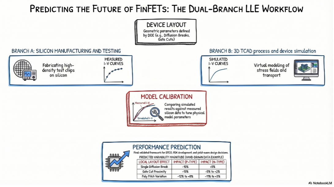
A useful TCAD model for LLEs cannot be judged only by whether it reproduces one transfer curve. The objective here was broader: to build a framework that could explain measured behavior across multiple layout-dependent scenarios and then be used to anticipate the impact of design or process changes. That is why the framework was validated against a dataset built from more than 30,000 silicon measurements, rather than against a narrow set of isolated reference structures.
The model was applied especially to Diffusion Break (DB) and Gate Cut (GC) sensitivity, but also to related geometry-dependent effects such as poly pitch and fin pitch. It needed not only to reproduce the correct trend direction, but also to capture the asymmetry between p-type and n-type devices. The data show that p-type FinFETs exhibit significantly stronger sensitivity, with stress-related variations reaching roughly ±12%, while n-type devices generally show smaller shifts (often below 5%) and sometimes more non-monotonic behavior because different stress components compete with one another.
This distinction is important because it reveals what the model is really trying to capture. The challenge is not simply to predict that “more stress means more current.” The challenge is to reproduce a physically anisotropic and carrier-dependent system in which the sign and magnitude of the electrical response depend on the detailed orientation and decomposition of stress inside the device. That requires the framework to be both mechanically detailed and electrically calibrated.
3. How Do We Build a Process-Aware 3DFinFET Structure?
The starting point of the modeling flow is a 3D process/device representation of the FinFET, constructed so that the most relevant layout-sensitive process features can be included explicitly. The model does not attempt to reproduce full wafer-scale variability or the complete fabrication line. Instead, it focuses on localized process variability and local geometry effects, because those are the mechanisms most relevant to stress-related LLEs.
That localization is deliberate. The goal is not to simulate every possible source of variation, but to build a model with enough process realism to capture how specific layout choices—such as a diffusion break configuration or a gate cut position—alter the local stress state and therefore the electrical behavior of the device. This required the inclusion of embedded epitaxial regions, gate stack materials, dielectric and isolation structures, and the thermal history needed to generate the final stress condition. The framework also incorporates the anisotropic stress response of Si/SiGe materials, which is essential for tracking how strain propagates into the channel.
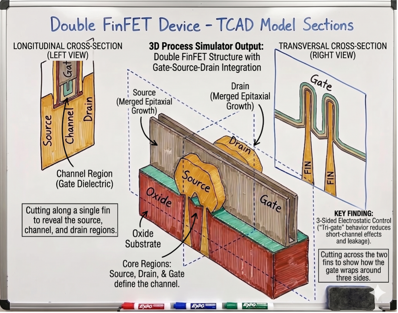
In practical terms, the framework sits between two engineering layers. It is far more physically detailed than a compact model but still focused enough to be useful for layout sensitivity studies and technology exploration. That middle ground is exactly what makes it effective for layout-aware variability analysis and DTCO-oriented studies.
4. Why Was the Calibration Organized in Two Distinct Phases?
One of the most important choices in the modeling flow was to organize calibration in two phases: first process calibration, then electrical/device calibration. That separation matters because stress-related LLE modeling becomes unreliable very quickly if structural assumptions are not anchored before the electrical fitting begins.
The process-calibration phase established the geometry and material representation of the reference transistor. The calibrated structure includes an effective oxide thickness (EOT) of about 7.7 Å, corresponding to a stack with approximately 6 Å of SiO₂ and 11 Å of HfO₂. Other structural assumptions were tuned to create a physically credible reference before the transport fitting began. Subthreshold behavior was then adjusted using interface-trap-density assumptions, while drain current was calibrated through parameters such as fin height and an electrical gain factor.
This sequencing protects the model from degenerating into pure curve fitting. If the process representation is unstable, electrical parameters can always be forced to match measured curves, but the result may no longer correspond to a physically plausible device. By separating structural calibration from transport calibration, the final model remains much more defensible as a predictive engineering framework.
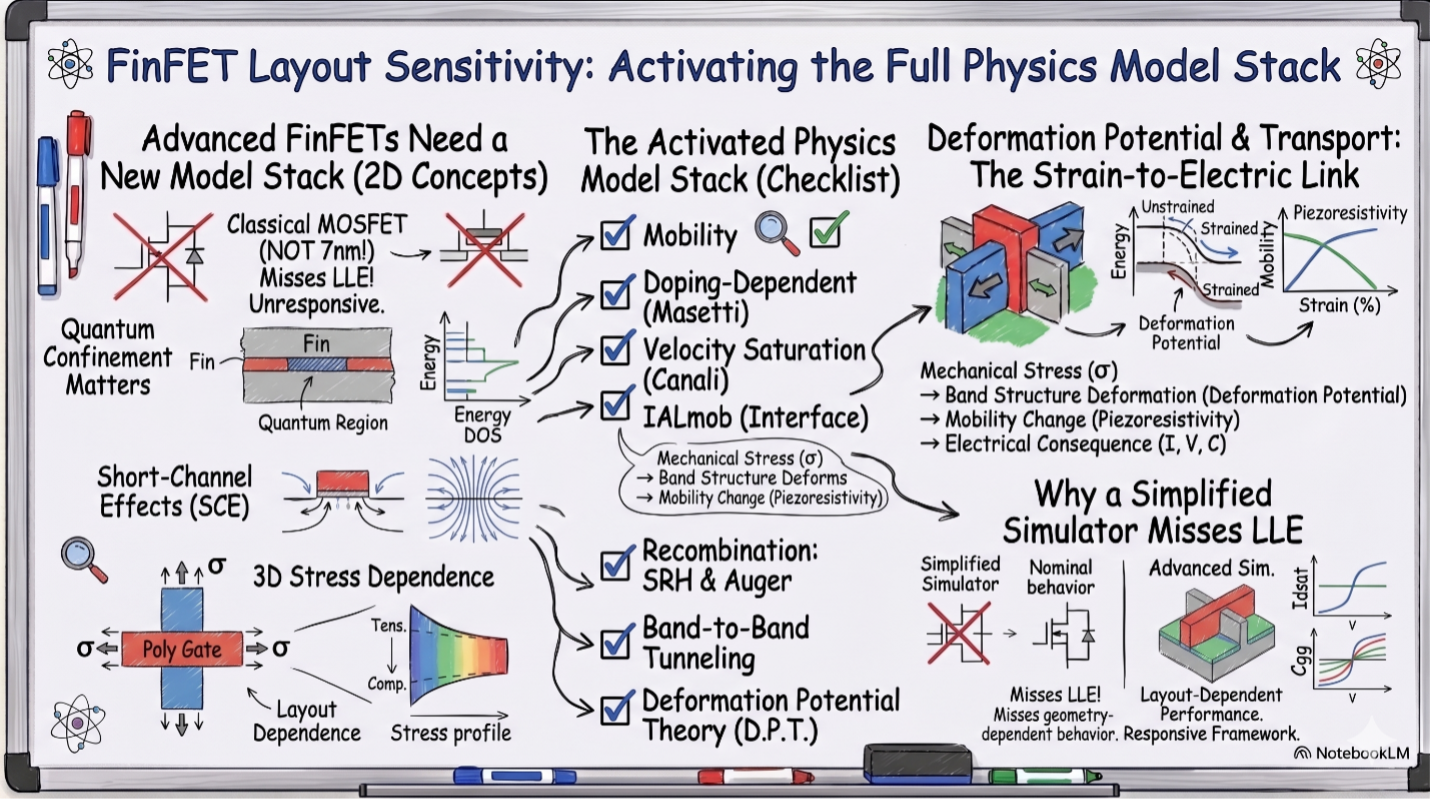
5. What Does the Physics Stack Inside the Simulator Look Like?
Once the reference structure was established, the next step was to activate the physical models needed to reproduce advanced FinFET behavior under stress. The simulator setup includes Masetti doping-dependent mobility, Canali velocity saturation, IALMob, piezoresistive mobility, Shockley–Read–Hall (SRH) recombination, Auger recombination, band-to-band tunneling, deformation potential theory, density-of-states corrections, and a density-gradient quantum correction.
This model stack reflects the fact that the target problem is not a classical long-channel MOSFET. At a 7nm-class FinFET node, subthreshold electrostatics, mobility degradation, quantum confinement, and stress-sensitive transport all matter, and they interact inside a three-dimensional geometry. The use of deformation-potential-based physics and piezoresistive mobility correction is particularly important, because these are the mechanisms that translate mechanical stress into electrical consequence.
These models were not included for completeness alone. They were necessary because the target problem is inherently layout sensitive. A simplified simulator might reproduce nominal transistor behavior while completely missing the sensitivity that appears when local geometry changes. The full stack makes the framework responsive to the very effects it is trying to explain.
6. Why Was Stress Tensor Decomposition the Real Key?
At the center of the entire framework lies one idea: not all stress is equivalent. A single scalar stress value is not enough to explain the observed behavior of modern FinFETs, especially when the measured sensitivities differ so strongly between n-type and p-type devices. The analysis therefore decomposes the stress field into its major components—especially longitudinal, vertical, and transversal stress and studies how each of them contributes to the electrical response.
This decomposition is what makes the PMOS versus NMOS asymmetry physically understandable. The results show that longitudinal stress is the dominant contributor to p-type layout sensitivity, which explains why PMOS devices can show such strong dependence on Diffusion Break and Gate Cut configurations. For n-type devices, the picture is more complex: vertical and transversal stress components can become more relevant, and the net electrical response is often smaller and less monotonic because several components partially compete with one another.
That is one of the most interesting lessons of the entire modeling effort. The stronger PMOS sensitivity is not merely an empirical observation from measurements; it becomes a physically interpretable consequence of how different carriers respond to different stress orientations inside the 3D device structure. This is exactly the kind of insight that TCAD can provide and measurements alone cannot easily reveal.
7. How Did Silicon Validation Prove the Model’s Credibility?
A TCAD framework matters only if it reproduces what silicon actually does. The 3D model was therefore calibrated and then validated against the high-density measurement dataset, with special attention to the layout scenarios that matter most for stress-related LLEs. The agreement between simulation and measurement is strong for both PMOS and NMOS devices, and the framework reproduces the main trends associated with Diffusion Break and Gate Cut sensitivity.
This validation step is especially important because the target effects are not always large. In some cases, the shifts are only a few percent, particularly for n-type devices. Reproducing both the larger PMOS sensitivity and the smaller, more complex NMOS response is therefore a meaningful test of model credibility. It shows that the framework is not just fitting one nominal device but is capturing the correct layout-dependent physics across different device polarities and configurations.
That same validation is what later enables the framework to be used for broader process studies. Once the model is shown to reproduce measured layout sensitivity, it becomes possible to explore things like gate-cut timing, dielectric isolation choices, SDB trench width, spacer thickness, and temperature, all of which would be much harder to isolate experimentally across every combination.
8. How Does Stress Physics Translate into Compact Models?
One of the most valuable aspects of the framework is that it does not stop at stress simulation. The extracted sensitivities are explicitly mapped into BSIM-CMG-relevant compact-model parameters, including U0, UA, DVTP0, DVTP1, DVTP2, and LPE0. This step is important because it translates a physics study into something that can directly influence circuit simulation and design flows.
That mapping is where the broader importance of the work becomes especially clear. If the results remained only inside TCAD, they would be useful for understanding device physics but much less useful for design enablement. By connecting stress-induced layout sensitivity to compact-model parameters, the framework creates a path from layout-sensitive device behavior to SPICE-compatible circuit impact. That bridge is exactly what is needed for PDK development, DTCO, variability-aware simulation, and yield-oriented design analysis.
This reinforces one of the main messages of the whole series: in advanced nodes, layout is not just a drawing artifact. It is a physical boundary condition that must eventually be represented in the model designers use every day. The compact-model mapping is what makes that possible in practice.
9. What New Capabilities Did This Framework Unlock?
Once calibrated and validated, the framework became much more than a device simulator. It became a way to ask “what if?” questions that matter directly in advanced-node technology development. The model was used to evaluate the impact of gate cut strategies, spacer deposition choices, dielectric isolation materials, SDB trench width changes, spacer thickness variability, and temperature, showing how each of these process or layout knobs can alter the magnitude, and sometimes even the sign, of stress-related LLE behavior.
Some of these results are particularly striking. The analysis shows that Gate Cut timing can strongly affect stress sensitivity, that dielectric isolation materials can significantly improve or degrade PMOS performance, that SDB over-etching penalizes PMOS much more strongly than NMOS, and that increasing temperature from 300 K to 375 K attenuates LLE sensitivity by about 80% for n-type devices and 40% for p-type devices. These are not abstract observations; they show how the framework can guide real trade-offs in process and integration development.
That is one of the most practically meaningful aspects of the model. It transforms measured silicon variability into actionable process insight, which is one of the clearest forms of value that TCAD can deliver in an industrial semiconductor context.
10. What Are the Inherent Limits of the Current Framework?
A credible modeling framework has to define not only what it can do, but also what it cannot do. The model does not attempt to simulate full wafer-scale variability, and some of its process assumptions remain constrained by the proprietary nature of the underlying technology. The focus is on localized process variation, local geometry perturbations, and stress-related electrical sensitivity, rather than on reproducing every possible source of manufacturing variability across the full fab environment.
There are also limits related to node and foundry transferability, measurement noise, simplified stress representation, static geometry assumptions, and computational cost. These are not secondary caveats. They define the realistic scope of the framework and make clear that it should be understood as a powerful but bounded engineering tool. It can explain and predict a large class of layout-dependent effects, but it is not a universal replacement for silicon characterization or full manufacturing variability analysis.
In practice, that is one of its strengths. The framework is ambitious without being vague. It is built for a specific problem, stress-related Local Layout Effects in advanced FinFET devices, and it addresses that problem in a way that remains physically grounded and practically useful.
Conclusion
If the previous post was about how stress-related Local Layout Effects were measured, this one is about how those measurements were turned into predictive physics. A useful LLE model must do more than fit electrical curves. It has to connect local geometry, process-induced stress, anisotropic carrier transport, and measured device response inside a framework that is both physically coherent and experimentally validated. That is exactly what the 3D TCAD flow was built to do.
By combining a process-aware 3D FinFET structure, a two-phase calibration flow, a rich transport and stress-physics model stack, and validation against high-density silicon measurements, the framework provides a predictive basis for understanding layout-dependent variability in a commercial 7nm FinFET technology. It also creates a bridge from device-level stress physics to compact-model parameters, making the work directly relevant to PDK development, DTCO, process optimization, and variability-aware design.
And once such a model exists, the most interesting question becomes the next one: what does silicon actually reveal about the strongest LLE mechanisms? That is where the discussion naturally goes next.
What Comes Next
In the next article, we will move from the modeling framework to the main results: how Diffusion Breaks, Gate Cuts, Poly Pitch, and Fin Pitch affect electrical behavior in measured 7nm FinFET structures, why PMOS devices are so much more sensitive than NMOS, and what the combined measurement-and-TCAD analysis reveals about the underlying stress physics.