

In the first post of this series, I introduced the central problem: in advanced CMOS technologies, transistor behavior is no longer determined only by nominal dimensions. The surrounding layout matters. Neighboring features, local geometry, and process-dependent stress fields can all perturb the channel and create systematic variations known as Local Layout Effects (LLEs). In modern FinFET nodes, these effects have become relevant for variability, compact modeling, DTCO, and yield-aware design.
That naturally raises a harder question: how do you actually measure LLEs on silicon? If two transistors differ electrically, how do you know whether the cause is local stress, gate-edge proximity, parasitic resistance, process fluctuation, or simple measurement noise? In other words, how do you isolate the effect of layout context without mixing it up with everything else happening inside an advanced technology node?
The answer starts with experimental design. The work relies on a high-density characterization chip fabricated in a commercial 7nm FinFET process, containing more than 30,000 devices under test (DUTs). Those devices are arranged in carefully structured modules designed to isolate specific layout-dependent mechanisms. The overall methodology combines a Design of Experiments (DOE) strategy, layout-controlled test structures, automated electrical characterization, and statistically robust data analysis. The goal is not simply to measure many devices, but to separate individual LLE contributions in a way that can later be modeled and predicted.
This post focuses on that experimental methodology: how the chip was organized, why specific electrical observables were chosen, how the DOE was built, and how the measurement flow was structured to separate real layout-driven behavior from background variability.
1. Why Is Isolating Variability So Difficult?
Studying Local Layout Effects experimentally is difficult because transistor variability at advanced nodes is never caused by a single mechanism. In a real FinFET technology, electrical characteristics can be influenced by stress, lithographic interactions, local pattern density, well proximity, doping-related perturbations, work-function variation, parasitic resistance, and broader process fluctuations. If the goal is to isolate one specific effect, such as Diffusion Break proximity or Gate Cut placement, then the experimental flow must be built so that the layout-dependent contribution becomes visible without being buried under everything else.
That is why the measurement strategy is based on controlled differentiation: vary one layout attribute at a time, keep the surrounding conditions as stable as possible, replicate structures across the chip, and use statistical aggregation to expose systematic trends. The objective is not merely to observe variation, but to decompose it.
This is especially important for stress-related LLEs. Mechanical stress is not directly visible in an electrical measurement. It has to be inferred from how device parameters shift when local geometry changes in a controlled and repeatable way. That makes experimental design just as important as the electrical measurements themselves.
2. How Was the Test Chip Built to Isolate Specific Effects?
The characterization platform is a high-density test chip implemented in a commercial 7nm FinFET technology, with more than 30,000 DUTs distributed across dedicated structures. That scale matters. If the objective is to isolate subtle but systematic layout effects, then a handful of devices is not enough. You need enough replication to compare multiple layout contexts, enough control to maintain meaningful local environments, and enough statistical depth to distinguish deterministic behavior from random spread.
The chip was therefore organized using a modular characterization strategy. Instead of trying to measure every possible source of variability at once, the layout was partitioned into dedicated blocks targeting specific LLE categories. Separate modules were built to investigate Diffusion Break proximity, Gate Cut proximity, well or p–n boundary effects, fin pitch, and poly pitch. This modularity is one of the strongest features of the methodology because it allows each mechanism to be examined in relative isolation before more complex interactions are considered.
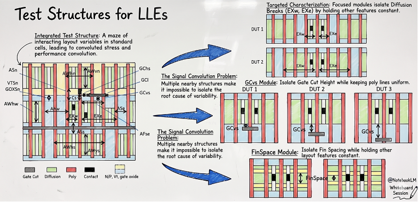
The local environments around the DUTs were carefully controlled so that comparisons between structures remained meaningful. The aim was not to mimic arbitrary product layouts, but to create representative and repeatable local neighborhoods in which a single geometric parameter could be varied and its electrical consequence observed. That principle sits at the center of the entire methodology.
3. What Is the Role of the Design of Experiments (DOE)?
At the core of the measurement flow is a layout-aware Design of Experiments (DOE). The guiding principle is straightforward: if a particular layout feature is suspected to influence transistor behavior, then that feature must be varied in a controlled way while the rest of the local environment is kept as constant as possible. In practice, this means designing families of structures where one geometric parameter changes and the surrounding conditions remain fixed.
That approach was used to partition the major layout-dependent mechanisms into smaller, manageable sub-problems. Dedicated modules were created to study how the device responds when placed near a Diffusion Break, near a Gate Cut, or under different fin pitch and poly pitch conditions. By comparing DUTs that differ only in one targeted feature, the methodology makes it possible to attribute shifts in current, threshold voltage, or subthreshold behavior to a specific geometric cause rather than to uncontrolled background variation.
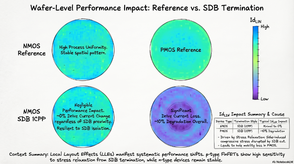
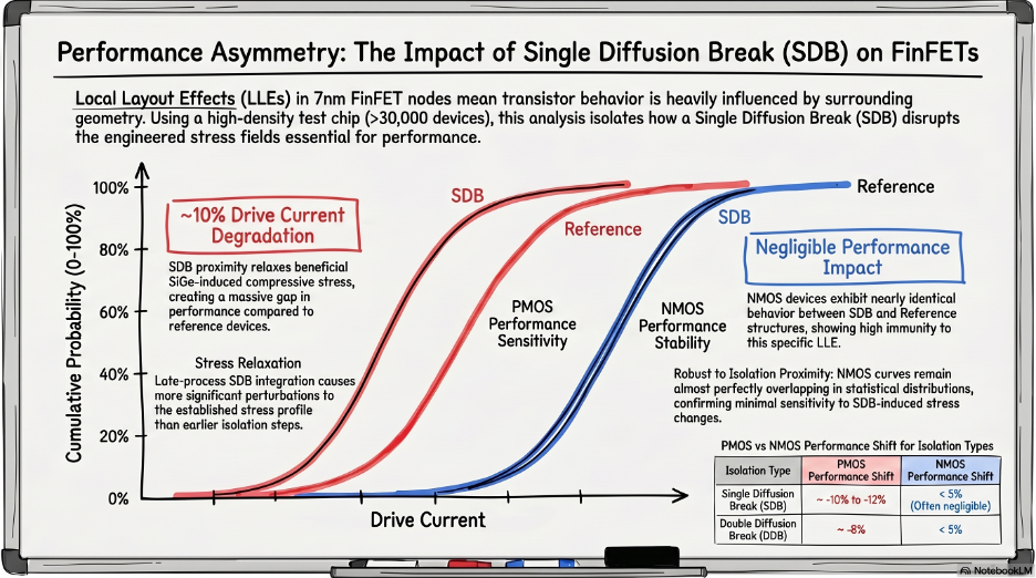
Replication was built in from the beginning. The same design ideas were repeated across device types and threshold-voltage flavors, making it possible not only to identify the presence of an effect, but also to understand how strongly it depends on device polarity and operating regime. This is one of the reasons why the data clearly show that p-type devices are significantly more sensitive to stress-related layout perturbations than n-type devices.
4. Why Is Linear-Region Current the Best Stress Monitor?
Not every transistor parameter is equally useful when the goal is to monitor stress-related variability. A strong emphasis was placed on electrical quantities derived from Id-Vgd measurements, especially in the linear regime. That choice is physically motivated: carrier mobility is highly sensitive to mechanical stress, and in the linear region the drain current provides a more direct and analytically accessible view of mobility-related changes than in deep saturation, where velocity saturation and other nonlinear effects play a larger role.
This is why linear-region drain current was used as one of the primary observables for stress monitoring. It offers a useful balance between physical interpretability, reduced parasitic sensitivity, and measurement stability. In practical terms, it becomes an experimental bridge between the electrical data and the later physical interpretation based on local stress and mobility perturbation.
The characterization flow nevertheless uses a broader set of parameters. Measurements were taken in both linear and saturation conditions, and the extracted metrics included Ioff, Ion, Vt, subthreshold swing, and additional current- and resistance-related quantities. This richer set is important because not all LLE mechanisms manifest in the same way: some primarily perturb mobility, others shift threshold voltage, and others change parasitic or short-channel behavior more indirectly.
5. Test Structures Matter Too: Why PMA Was the Right Choice?
The methodology depends not only on the layout of the devices, but also on the design of the measurement structures used to access them. Several forms of test infrastructure were evaluated, including Single Padded structures, Passive Arrays, Active Arrays, and Passive Matching Arrays (PMA). Among these, PMA emerged as the preferred solution because it provided the best combination of area efficiency, measurement accuracy, and reliability.
This choice is more important than it may appear. In advanced-node characterization, the structure used for testing is itself part of the methodology. A structure that consumes too much area reduces the number of useful replications that can fit on the chip. A structure that is electrically noisy weakens the statistical quality of the results. A structure that does not preserve a controlled local environment makes it harder to attribute observed shifts to a specific LLE mechanism. PMA was selected because it supported more robust and scalable comparisons between nominally similar devices placed in different layout contexts.
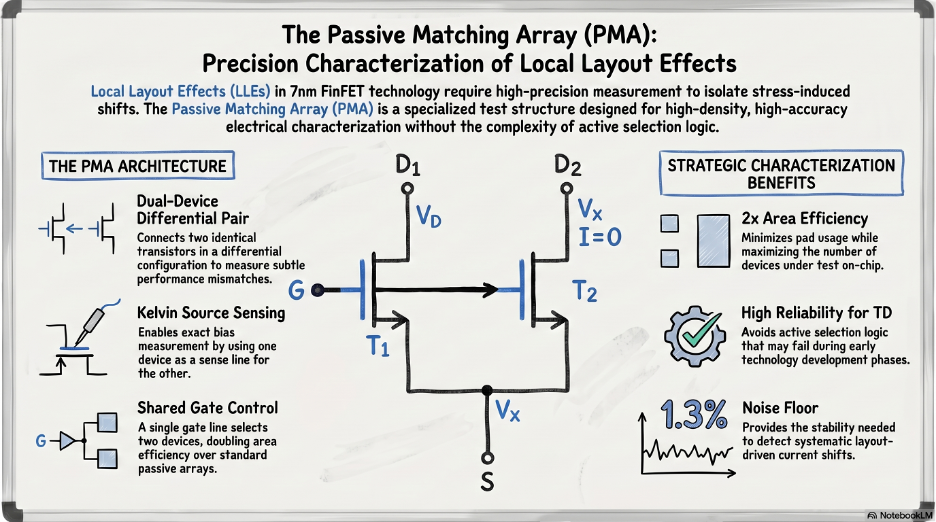
The PMA framework also enabled comparative measurements, which are especially useful for LLE analysis. These effects are often easier to identify when one DUT is compared directly against a nearly identical reference that differs only in one layout feature. That comparative logic runs throughout the entire methodology.
6. Why Was Automated High-Speed Characterization Essential?
Once the chip and DOE are defined, another challenge appears: scale. A test chip with more than 30,000 devices cannot be characterized efficiently with a manual workflow. The measurement campaign therefore relied on automated high-speed parametric testing, using industrial infrastructure that includes pdFasTest® for electrical acquisition and Exensio® for automated data ingestion and analysis. This moved the characterization flow from isolated measurements to a structured and repeatable data pipeline.
The measurements were based on Id-Vgs sweeps collected in both linear and saturation regimes, from which key electrical parameters were extracted. The analysis flow then combined measurement results with layout descriptors and spatial information, enabling the generation of CDFs, wafer maps, and parameter reports. This is important because LLE characterization always has to answer two questions at once: what is the local geometric effect, and how large is that effect compared with broader wafer-level or process-level variability?
Automated extraction also made it possible to evaluate thousands of related structures in a consistent way. That consistency becomes crucial when some of the effects being studied are only a few percent in magnitude. Without standardized acquisition and reporting, it would be much harder to know whether a small trend is physically meaningful or simply the result of inconsistent analysis.
7. How Was Statistical Robustness Guaranteed?
One of the strongest features of the methodology is that it was built with statistical robustness in mind. Device parameters were analyzed using median values, and the observed standard deviation remained below roughly 1.3% for drain current and below about 1.6% for threshold voltage and subthreshold swing across the experiments. Those numbers are important because they define the background noise floor against which systematic LLE shifts must be detected.
This is one reason why it becomes possible to make credible claims about layout-induced effects of several percent and, in p-type devices near certain layout features, even above 10%. Once the background variability is quantified and controlled, the observed shifts become interpretable as physical signals rather than anecdotal scatter. The strength of the methodology does not come only from measuring many devices, but from measuring them in a statistically disciplined way.
This emphasis on medians, replication, and controlled comparison also matters for the modeling work that follows. A predictive TCAD or compact-model framework is only as good as the data used to calibrate it. If the experimental baseline is noisy or poorly structured, the model may appear to fit but still lack physical credibility. The measurement methodology was explicitly designed to avoid that trap.
8. How Do Measurements Feed Physical Interpretation?
A key strength of the methodology is that it does not stop at electrical observation. The entire characterization flow was designed from the beginning to support physical interpretation and later model calibration. That is why the test structures were chosen not only for electrical readability, but also for compatibility with 3D TCAD-based stress simulation. The experimental side and the modeling side were built to support each other.
This point is central. A purely empirical measurement campaign can tell you that one layout performs better or worse than another, but it does not necessarily tell you why. By contrast, the methodology here was built so that electrical trends observed on silicon could be linked back to physically meaningful variables such as stress tensor components, mobility perturbation, and geometry-dependent process interactions. That is what later makes it possible to move beyond observation and toward prediction.
That is also why the main characterization targets, especially Diffusion Break and Gate Cut effects, were selected so carefully. These are not arbitrary layout features. They are exactly the kinds of structures that modify local stress boundary conditions in advanced FinFET integration and therefore create a direct bridge between layout, process, and measurable electrical behavior.
9. What Did This Experimental Methodology Ultimately Enable?
This experimental framework ultimately enabled several important outcomes. First, it provided a structured way to separate individual LLE contributions on silicon. Second, it produced data robust enough to support 3D TCAD calibration and validation. Third, it established a practical path from layout geometry to electrical sensitivity that is directly relevant to PDK development, DTCO, and process optimization.
This is one of the most valuable aspects of the whole approach: the methodology is not only academically rigorous, but also industrially useful. It is designed to answer questions that matter in a real technology-development flow: Which layout features generate harmful stress perturbations? Which devices are most vulnerable? How large are the shifts? Can the behavior be predicted before product design is finalized? And can those predictions be translated into actionable guidance for designers and technologists?
In that sense, the characterization methodology is not just an experimental foundation, it is what makes the later modeling and interpretation credible. Without a robust way to isolate LLEs on silicon, any attempt at predictive modeling would remain speculative.
Conclusion
If the first post of this series was about why stress-related Local Layout Effects matter, this second post is about how they can be measured in a meaningful way. The key message is that LLE characterization in an advanced FinFET node cannot rely on ad hoc transistor measurements. It requires a dedicated experimental architecture: a large and carefully structured test chip, a DOE that varies one layout feature at a time, robust electrical observables, automated analysis, and enough statistical discipline to distinguish real systematic effects from background variability.
That combination, more than 30,000 DUTs, modular layout-aware structures, high-speed parametric testing, and statistically controlled extraction, creates a solid foundation for understanding stress-related LLEs in 7nm FinFET technology.
And once that experimental foundation exists, the next question becomes unavoidable: how do you turn these silicon observations into a physical and predictive model? That is where TCAD enters the picture.
What Comes Next
In the next article, we will move from experimental characterization to model construction: how a 3D TCAD framework was built and calibrated to reproduce the measured behavior, how local stress tensors were extracted, and how the electrical impact of layout-induced stress was translated into a predictive modeling flow.