
For decades, the progress of CMOS technology was driven by two remarkably powerful ideas. Moore’s Law captured the exponential growth of transistor density, while Dennard scaling explained why shrinking transistors could simultaneously improve performance, reduce power, and cut area. In that historical regime, scaling delivered a rare combination of benefits almost “for free.”
That regime is now behind us. As CMOS entered the deep nanoscale era, geometric shrink alone stopped being sufficient to guarantee the classical power-performance-area (PPA) gains. Physical scaling continued, but with diminishing returns, and progress increasingly depended on architectural innovation, process integration, and Design-Technology Co-Optimization (DTCO). In other words, transistor behavior could no longer be understood from nominal device dimensions alone.
One of the most important consequences of that shift is that the surrounding layout itself has become part of the device. In advanced FinFET technologies, the local geometric environment around a transistor can measurably alter its electrical behavior through stress, electrostatics, and process-dependent interactions. Among these effects, stress-related Local Layout Effects (LLEs) have emerged as a particularly important source of systematic variability.
This topic is the focus of this PhD research, which investigates stress-induced LLEs in a commercial 7nm FinFET technology using a combined experimental and modeling framework. The work is based on a high-density test chip with more than 30,000 devices, a dedicated Design of Experiments (DOE) methodology to isolate layout-dependent effects, and a 3D TCAD flow calibrated against silicon measurements. In p-type devices, some layout-dependent stress perturbations were found to produce performance variations exceeding 10%, highlighting how strongly local geometry can influence transistor behavior in advanced nodes.
This first post sets the stage for the series. It explains why stress-related LLEs have become so important, how they connect to the end of “happy scaling,” and why they now sit at the intersection of device physics, compact modeling, DTCO, and yield-aware design. The posts that follow will go deeper into the measurement methodology, the modeling framework, the main silicon results, and the implications for future FinFET and GAA technologies.

1. Why Did “Happy Scaling” Give Way to a Harder Reality?
The historical promise of CMOS scaling was simple and powerful: make transistors smaller, and circuits become denser, faster, and more energy efficient. Under ideal Dennard scaling, a representative linear shrink by a factor of 0.7 reduced transistor area to about half while also improving delay and lowering dynamic power. This combination became the foundation of the classical PPA view of technology scaling.
But this favorable regime gradually weakened as transistor dimensions moved into the deep nanoscale domain. Once short-channel effects, leakage, and supply-voltage constraints became dominant, further gains could no longer be extracted by geometric shrink alone. At that point, continued progress relied more heavily on process boosters, new materials, more complex device structures, and increasingly aggressive co-optimization between technology and design.
This shift is not merely a historical footnote. It explains why variability mechanisms that were once secondary now become central. In a world where margins are tighter, device structures are three-dimensional, and layout compaction is aggressive, seemingly minor geometric details can propagate into measurable electrical differences. That is exactly the environment in which Local Layout Effects become critical.
2. Why Does Mechanical Stress Matter So Much in Advanced Nodes?
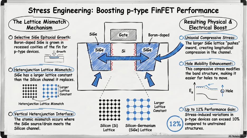
Mechanical stress has long been one of the most useful, and most subtle, physical levers in advanced CMOS. For the stress levels relevant to strain engineering, silicon remains in the elastic regime, meaning that mechanical deformation modifies the semiconductor band structure in a reversible way without introducing permanent crystallographic damage. The most important electrical consequence is a change in carrier mobility.
That mobility response is not isotropic. In silicon, the effect of stress depends strongly on crystal orientation, current direction, and carrier type. This is particularly relevant for (100)-oriented wafers, which are widely used in advanced FinFET logic technologies. Electrons and holes do not respond to stress in the same way, and this asymmetry is one of the reasons why strain engineering became such an important tool in CMOS optimization.
In practical terms, p-type devices are often more sensitive to stress-induced mobility changes than n-type devices. That point turns out to be central in the thesis as well: the silicon measurements and TCAD analysis show that p-type FinFETs are significantly more sensitive to local stress perturbations, with layout-dependent variations that can exceed 10% in specific configurations, whereas n-type devices typically show smaller and sometimes more complex responses.
So, stress is not only a background physical effect. It is both an opportunity and a liability: a tool that can be used intentionally to improve mobility, and at the same time a source of unwanted variability when it becomes coupled to layout context.
3. How Does Engineered Strain Turn Into Unintended Stress?
The semiconductor industry has intentionally exploited stress for years. Early strain-engineering approaches used lattice mismatch at the wafer level, for example, silicon grown on relaxed SiGe buffers, to induce beneficial global strain. These methods were effective in planar technologies and later in FD-SOI, but their efficiency became less straightforward in highly three-dimensional architectures.
To keep extracting mobility benefits in non-planar devices, the industry turned to more localized stress techniques. Examples include embedded epitaxial source/drain stressors, Contact Etch Stop Layers (CESL), and Stress Memorization Techniques (SMT). These approaches intentionally modify the local mechanical environment of the channel and are part of the broader toolbox that allowed CMOS to continue scaling after the breakdown of ideal Dennard behavior.
But once stress becomes a key ingredient of device optimization, an unavoidable question follows: what happens when the local layout unintentionally changes that stress field? This is where Local Layout Effects begin. Even when no additional “stressor” is purposely inserted by the designer, neighboring active regions, isolation structures, gate terminations, contact placement, and local pattern density can all perturb the stress distribution seen by the transistor channel.
This distinction between engineered strain and layout-induced stress variability is essential. One is intentional and beneficial by design; the other is context-dependent, often difficult to visualize directly, and can create measurable device-to-device differences even among transistors with identical drawn dimensions.
4. What Exactly Are Local Layout Effects (LLEs)?
Local Layout Effects are systematic, pattern-dependent variations in transistor electrical behavior that arise from the surrounding layout environment rather than from nominal dimensions alone. They can affect parameters such as threshold voltage, drive current, and subthreshold behavior. Unlike purely random variability sources, LLEs are deterministic in principle, which means they are not just “noise” but phenomena that can be characterized and modeled, provided the underlying physics and process dependencies are understood well enough.
In advanced FinFET technologies, several categories of layout features can act as LLE sources. The geometry of the active region and its proximity to neighboring structures can change the local stress field. Gate termination and line-end position can alter both electrostatic behavior and mechanical boundary conditions. Well-edge proximity can perturb local doping distributions, and contact placement can influence parasitic resistance while also disturbing nearby process-induced stress fields.
These interactions become substantially more complex in FinFETs than in planar devices because the channel is inherently three-dimensional and because the gate stack, source/drain integration, spacers, and isolation structures all contribute to a tightly coupled mechanical environment. In the thesis, the two most deeply investigated LLE mechanisms are Diffusion Break-related effects and Gate Cut-related effects, both of which were shown to modulate local stress and significantly affect device characteristics.
This is why LLEs are best understood not as an isolated modeling nuisance, but as an emergent property of modern device architecture and process integration. As devices become more three-dimensional and layout becomes more compact, the transistor increasingly “feels” its neighborhood.
5. Why Does DTCO Make LLEs More Important, Not Less?
Design Technology Co-Optimization (DTCO) has become one of the main ways to sustain density improvement once pitch scaling alone is no longer enough. Instead of relying only on smaller contacted poly pitch, fin pitch, or metal pitch, modern nodes increasingly achieve area gains by rethinking cell architecture, transistor placement, routing resources, and design rules together.
A representative example is the transition from Intel 7 to Intel 4, where the full density gain was not explained by pitch shrink alone. Intel combined physical scaling with DTCO-driven changes such as reduced standard-cell height, fin depopulation, and tighter diffusion separation, showing how modern density progress comes from both geometry and architecture.
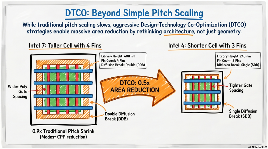
But these same strategies also exacerbate layout sensitivity. As diffusion breaks, gate cuts, isolation edges, and other neighboring features move closer to the active channel, their mechanical and electrical influence becomes stronger. Structures that once sat at relatively benign distances now fall inside the effective interaction zone of the transistor. In other words, the very techniques that help recover area scaling can also amplify LLEs.
This is one of the key messages of the thesis: DTCO and LLE sensitivity are tightly coupled. If layout compaction is pushed aggressively without understanding how local geometry modulates stress, the cost can appear later as unexplained variability, degraded matching, or reduced design margin. That makes stress-aware DTCO and LLE-aware compact modeling not optional refinements, but necessary ingredients of advanced-node development.
6. How Did FinFETs Solve One Problem Only to Expose Another?
The transition from planar MOSFETs to FinFETs was driven by the need to restore electrostatic control as scaling moved deeper into the nanometer regime. Multi-gate architectures offered much better control over the channel than planar devices, reducing leakage and extending CMOS scaling for another major generation.
However, the move to FinFETs also introduced a far more intricate mechanical environment. The fin geometry, gate stack, isolation, source/drain stressors, and local pattern density together create a three-dimensional stress landscape that is much harder to understand, and much harder to abstract, than in planar devices. The same architectural shift that improved electrostatics therefore made stress-related layout effects more structurally important.
Looking forward, the industry is moving toward Gate-All-Around (GAA) architectures such as nanosheet devices. GAA structures improve electrostatic control even further by surrounding the channel on all sides with gate material, and they enable current scaling through vertical channel stacking rather than continued horizontal fin multiplication. Intel’s RibbonFET and similar GAA approaches from other manufacturers reflect this transition.
At the same time, advanced interconnect innovations such as backside power delivery, for example, Intel’s PowerVia in 18A, are changing the layout and routing environment around transistors. In parallel, High-NA EUV is extending patterning capability by improving single-exposure resolution and overlay performance, with ASML reporting 8 nm resolution for 0.55-NA systems and imec/ASML demonstrating sub-20 nm pitch patterning in one exposure. These advances will enable further density scaling, but they will also make pattern fidelity, process control, and layout-aware variability even more important.
So although the device architecture is evolving, the central lesson remains the same: as scaling becomes more three-dimensional and more co-optimized, local context matters more. If anything, the problem becomes richer, not simpler, in the GAA era.
7. Why Is Predictive Modeling No Longer Optional?
Once LLEs become large enough to influence device current, threshold voltage, and eventually circuit timing or power, they must be represented in simulation. That means the effects cannot remain trapped inside process intuition or post-silicon debug: they need to be translated into SPICE-compatible compact models and variability-aware design flows.
A predictive framework for stress-related LLEs requires several tightly connected steps. First, the local stress field must be extracted through process-aware mechanical simulation with full stress-tensor resolution and realistic assumptions for the relevant strain sources, including epitaxial regions, gate materials, STI, and CESL. Second, that stress information must be translated into electrical impact through a piezoresistive mobility model that respects wafer orientation, current direction, carrier type, and device architecture. Third, those physical sensitivities must be abstracted into layout-aware compact-model parameters that designers can actually use at circuit level. Finally, the entire framework must be validated against dedicated silicon measurements specifically designed to isolate individual layout effects.
This is precisely the direction taken in this thesis. The work combines systematic measurement on a high-density 7nm FinFET test chip with a calibrated 3D TCAD framework, and it maps the resulting sensitivities into compact-model-relevant parameters such as mobility and threshold-voltage shifts. The objective is not only to explain observed behavior after the fact, but to build a predictive methodology that can support DTCO, PDK development, process tuning, and yield-aware design decisions.
As layout features move closer and process complexity increases, the value of such models only grows. In advanced nodes, accurate LLE characterization is becoming essential for variability prediction, design robustness, physical verification, and time-to-market.
8. The Core Thesis Behind the Thesis
If I had to reduce the entire research to a single statement, it would be this:
In advanced FinFET technologies, layout is no longer just a mask-level description of the device. It is part of the device physics.
That is why stress-related LLEs deserve attention. They connect transistor architecture, process integration, mechanical stress, compact modeling, and circuit-level variability in a single problem. They are also one of the clearest examples of how the end of “happy scaling” changed the semiconductor engineering mindset: performance is no longer improved only by shrinking features, but by understanding and controlling interactions that were once small enough to ignore.
In this work, the problem is addressed through a combination of silicon characterization, layout-aware DOE, stress simulation, and electrical modeling, with a strong focus on isolating physically meaningful effects and translating them into actionable design and process guidance. That combination is what makes the topic especially interesting: it sits exactly at the boundary between fundamental device physics and industrial usefulness.
Conclusion
The combined effects of aggressive DTCO, three-dimensional device architectures, and continued pitch scaling have transformed stress-induced Local Layout Effects from a secondary correction into a central design and modeling challenge. The strong directional dependence of carrier mobility on mechanical stress in silicon, together with the intricate stress distributions generated by modern FinFET process integration, makes accurate and experimentally validated LLE modeling indispensable.
In advanced CMOS technologies, LLE characterization is no longer optional. It has become a prerequisite for variability-aware PPA optimization and a key enabler of scaling beyond the traditional happy-scaling regime.
What Comes Next
In the next post, we will move from the “why” to the “how”: how do you experimentally isolate Local Layout Effects in a modern FinFET node without mixing together stress, electrostatics, and random variability? That will take us into the heart of the characterization methodology developed in the thesis: the test-chip architecture, the layout DOE, and the measurement strategy used to separate individual LLE contributions on silicon.