
Written by: Steve Zamek, Jon Holt, Sandy Chen
At APEC 2026 (Session IS02.1: AI and Digital Twins Transforming Power Device Innovation), our team presented two production-deployed AI/ML use cases drawn from more than a decade of experience with power semiconductor manufacturers. This post captures key lessons.
This blog post and presentation are part of a larger series of publications by this team on practical approaches in deploying AI/ML in semiconductor and power semiconductor manufacturing:
- End-to-End Yield Management for Compound Semi
- Predicting Yield Loss from Source: Machine Learning for Compound Semiconductor Manufacturing
- Transforming End-to-End Yield Management in Compound Semiconductor Manufacturing
Why Power Semiconductors Are Different?
AI-driven yield improvement has been well-studied in logic and memory manufacturing. But power semiconductors, SiC, GaN, IGBT, discrete silicon, present a uniquely challenging environment. The material mix is higher, defectivity levels are greater, and the manufacturing flow has more vertical integration: boule growth, substrate grading, epitaxy, multiple burn-in insertions, die attach, and module assembly. The manufacturing facilities are typically older and less mature with respect to traceability and data quality that mature silicon fabs largely solved years ago.
Eleven of the companies featured in Yole’s 2025 Power Electronics Industry report are active Exensio users, all of them for more than ten years. The two use cases we presented at APEC reflect what we’ve learned across those deployments.
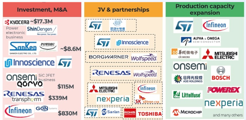
Source: Status of the Power Electronics, Yole 2025
Use Case 1: Substrate-Limited Yield in SiC
The Problem
Substrate quality is one of the dominant contributors to yield loss in SiC manufacturing. The question is: can you predict which substrates will limit yield, and act on that prediction before committing expensive downstream processing?
The Approach
The conventional method for identifying killer defects relies on the Kill Ratio metric: comparing yield between “clean” and “dirty” dies using a 2×2 confusion matrix. This method relies on die-level summaries for each defect class. In silicon, substrates are nearly defect-free, and most focus is on the inline defects introduced in the fab or foundry.
In compound semiconductors, the picture is more complex. You’re working across multiple inspection steps, bare substrates (pre- and post-epi) and patterned wafers (in-line).. Die level summaries do not apply well as die grid on unpatterned substrate is not defined. Also judging good/bad die on electrical wafer sort alone is insufficient. Power devices require high-current high-voltage tests under unique load conditions which often can’t be realized during the wafer sort.
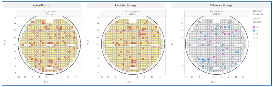
Our approach uses bare substrate and epitaxial defect data to train a predictive model that generates a predicted electrical bin map, a per-die, per-wafer classification of expected pass/fail outcome prior to electrical test. The model allows operators to grade substrates before committing them to the full fabrication flow. Furthermore, such a prediction can be performed for any virtual die size and enables a user to experiment with different die size to estimate yield.
Results
The results discussed below are based on our experience with silicon carbide substrate from multiple different suppliers. Nevertheless, the same approach can be applied to other types of semiconductors and are not limited to SiC. In production deployments, the model:
- Correctly identifies yield-limiting substrates consistent with published literature on SiC defect kill mechanisms
- Saves several percentage points of yield by enabling upstream substrate disposition decisions
- Generates actual vs. predicted vs. difference bin maps that make model behavior interpretable and auditable
The model also exposes four classification categories for each defect class:
- TP (True Positive): actual pass, predicted pass — correct disposition
- TN (True Negative): actual fail, predicted fail — correct disposition
- FP (False Positive): actual fail, predicted pass — underkill, a yield liability
- FN (False Negative): actual pass, predicted fail — overkill, a cost liability
Production Challenges
Moving from pilot to production exposed a variety of challenges.
Inspections: The same substrate may be measured on different inspection tools across different lots or material flows. Defect classification schemes differ between tools, and defect counts are not directly comparable without normalization. The inspection recipes are not mature and are constantly being revised.
Spatial registration: optical inspection on bare substrates uses global wafer coordinates. These coordinates need to be registered correctly with respect to die-coordinates. Many of the older fabs have no proper registration between global wafer coordinates and die coordinates. Furthermore, defects in non-cubic lattice semiconductors (e.g. SiC), can be large in size and cover more than one die. However, inspection scans have insufficient information to understand the spatial extent of these defects.
Probe + Burn-In: Poor data quality is an endemic — orientation errors, die offset between inspection and test coordinates, and inconsistent die ID conventions make spatial alignment non-trivial. This necessitates data cleansing and validation before a meaningful model can be built.
Module + Burn-In: Many manufacturers are struggling with end-to-end die traceability. . Cherry-picking and grading at the substrate level means that fab lots after epi may look completely different from lot composition before epi. By wafer sort, nearly every wafer in a lot may originate from a different pre-epi material lot. By module assembly, you’re tracking individual die across sub-assemblies.
Missing data: introduces an additional bias risk. If you simply discard records with missing inspection data, you are not discarding them randomly. You are more likely to discard records from specific tool types, time windows, or material grades, which systematically biases your training set. For example, missing data may often originate from inking out of bad dice in assembly. Discarding these dice means you are removing a large population of bad dice, therefore leading to an overly optimistic model (aka “underkill”).
Use Case 2: Predictive Die Binning for Assembly
The Problem
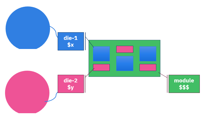
Power modules, e.g. automotive traction inverters, are very expensive parts assembled from multiple dice sourced from multiple wafers, often multiple products and multiple vendors. Quality escapes, where bad die is assembled into a module are very expensive. The question is: can you predict final test outcome from wafer sort data, and use that prediction to optimize die disposition before assembly?
This is not unique to power semiconductors. High-end compute modules (MCMs for data centers) face the same challenge. Both contain tens of die per module. In both cases, the cost of a module failure propagates across the assembly cost of every die in that module.
The Approach
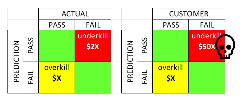
The goal is to build a binary classifier (pass/fail at module final test) trained on wafer sort parametric data and then optimize the classification threshold not for accuracy but for the final module cost.
Why cost, not accuracy? Because underkill and overkill have highly asymmetric costs. Sending a die that will fail module test to assembly wastes the entire module assembly cost, potentially $50x the individual die cost. Overkilling a good die wastes only that die alone ($x). The optimal classifier is the one that minimizes total expected cost given those asymmetric consequences.
Real-World Complexity
Real-world deployment of this type of solution is very complex:
- Messy and missing data: Real bin maps and parametric maps in production may be spatially distorted, incompletely tested, or corrupted by data transformations. This is due to the fact that the tester and the prober get programmed by different engineering functions. While it’s the prober’s task to land on the right die on the wafer, the tester is focused on running the test program. As a result, the output of the tester will often have incorrect die size, coordinates and even wafer orientation.
- Multiple test insertions: Wafer probe, wafer burn-in, module assembly test, module burn-in, final test, each with its own data format, limits, and binning conventions. This poses multiple questions. What’s the ground truth of good vs bad die? What to do about dice that tested good but got inked out and never made it to the subsequent test due to some spatial outlier screening (e.g. GDBN)?
- Modules with tens of die: Different products, different lots, different fab processes, each requiring its own predictive model, with its own traceability requirements. Modules with tens of dice make the model training explode. Training such a model requires a compute infrastructure, that many manufacturers cannot afford.
- Multiple sub-assemblies: Parts go through a tiered subassembly process, where a part assembled and tested at one step becomes the starting material for the next sub-assembly at the higher integration level. This poses the question – what is the optimization target? Now each subassembly step requires its own decision (classification), but the ultimate target is the combined cost of all sub-assembly steps. The complexity grows dramatically with the number of sub-assembly steps.
- Poor traceability: In power semiconductor manufacturing, die traceability from wafer to module requires explicit engineering effort, it is not automatic
Our production deployments go to significant lengths to ensure that all data across all manufacturing operations is aligned, traceability is maintained, and datasets are analytics-ready before any model training begins. Nevertheless, building, validating, deploying, and maintaining such models remains a challenge.
The Data Infrastructure Imperative
Both use cases point to the same underlying challenge: getting the data analysis-ready. It was reported by multiple customers that data preparation and validation is up to 90% of the engineering effort required to successfully use these models in production.
Manufacturing data in the power semiconductor industry is genuinely fragmented. For fabless companies, dice are coming from different vendors, they go to different OSAT’s and it becomes a huge undertaking to gather all that data in a single platform. One may think vertically integrated device manufacturers, with in-house manufacturing, face an easier task. However, that is far from reality. While the data may belong to the same company, it is distributed across multiple sites and a variety of systems – MES, ERP, QMS, FDC, and SPC systems; often different systems at different sites. Each such system becomes a a silo, that’s where enterprise-wide deployment of a yield management platform such as Exensio becomes crucial.
As an example of such a deployment, let us consider onsemi. At PDF Solutions Users Conference in December 2025, onsemi’s Tom Grein presented how onsemi use Exensio as a single platform and ground source of truth across their entire SiC manufacturing flow: from silicon carbide powder through crystal growth, epitaxy, device fabrication, and module assembly. Their genealogy chain tracks: Boule growth → Substrate → Epitaxy → Fab Wafer → Module. That kind of end-to-end data infrastructure is not a nice-to-have. It is the prerequisite for any serious analytics.
Call to Action: Make Your Data AI-Ready
Based on 10+ years of production deployments with power semiconductor manufacturers, here is what it takes to build the foundation for a successful AI strategy:
- Establish manufacturing IT infrastructure. You cannot run AI models on data that doesn’t exist in a usable form. Invest in data collection, storage, and access infrastructure comes first.
- Break data silos. Consolidate all manufacturing data, materials, inline wafers, inline equipment, assembly, and test, in a single platform. Data that cannot be joined is data that cannot be modeled.
- Clean the data at the source. Ideally, data quality is enforced at the point of collection. If such a step isn’t possible, establish an enterprise “data cleaning layer” that standardizes formats, validates values, and flags anomalies before data enters the analytics environment.
- Standardize across sites and material flows. SEMI standards do not provide sufficient standardization to meet the challenges of data analytics. Manufacturers need to establish their own data standards for each data domain and enforce them consistently across sites and material flows.
- Establish supply chain traceability. High mix of products in power semiconductors results in diverse material flows. It becomes a combination of fully in-house, partially outsourced and fully outsourced (turn-key) flows. From raw materials to shipped modules, it is no small task to trace any die from a shipping module to the starting material. However, the materials in the world of power semiconductors are often what makes the difference between good module and one that gets back from the field.
These five steps are prerequisites to driving manufacturing excellence. AI models trained on incomplete, misaligned, or biased data will produce misleading results, and in a production disposition system, misleading results have direct cost consequences.
The semiconductor industry’s AI transformation is well underway. The manufacturers who will capture the most value are not necessarily those with the most sophisticated models. They are the ones who have done the unglamorous work of making their data fit to learn from.
This post is based on the APEC 2026 presentation “Advanced Analytics and AI to Improve Semiconductor Cost and Quality” (Session IS02.1), presented by Steve Zamek, Jon Holt, and Sandy Chen of PDF Solutions on March 24, 2026.