

The earlier posts in this series moved step by step through the problem of stress-related Local Layout Effects in advanced FinFET technologies: why they matter, how they can be measured, how they can be explained through calibrated 3D TCAD, and how both layout features and process-integration choices can amplify or attenuate their impact. At this point, the most important question is no longer what causes the effect, but what can actually be done with that knowledge. That is where the work becomes especially interesting: once layout-dependent stress sensitivity is understood and modeled, it stops being just a device-physics topic and becomes a design-enablement topic.
That transition is the real value of the whole effort. A measured or simulated LLE trend is useful on its own, but its practical significance depends on whether it can influence compact models, PDK assumptions, DTCO decisions, layout guidance, and ultimately yield-aware circuit design. The work described throughout this series was built with exactly that objective in mind: not only to explain stress-induced variability in a 7nm FinFET technology, but to connect that understanding to the kinds of engineering decisions that matter in a real technology-development flow.
This final post focuses on that broader engineering picture. It looks at how the modeling framework can be translated into SPICE-relevant compact-model parameters, how the results can support PDK and DTCO development, what the main limitations of the current framework are, and where the work can evolve next, especially toward AI/ML-assisted modeling, compound LLE analysis, and future GAA architectures.
1. Why Is Predictability the Real Deliverable?
At advanced nodes, variability is not just a matter of post-silicon curiosity. It affects whether a design closes, how much margin is required, how robust standard cells remain across corners, and how much time is lost chasing layout-sensitive behavior late in the flow. This is why predictability matters more than raw explanation. A technology team does not just need to know that Diffusion Breaks and Gate Cuts perturb PMOS behavior; it needs to know whether those perturbations can be anticipated early enough to influence design rules, compact models, and process decisions.
That is one of the strongest outcomes of the work: the combination of silicon characterization, structured DOE, and calibrated TCAD creates a framework that is not purely descriptive. It supports a predictive view of stress-related LLEs, making it possible to estimate how layout and process choices will affect electrical behavior before those choices become costly product issues. That predictive angle is what turns device-level insight into something that matters for a full technology-development organization.
In practical terms, this means moving from statements like “PMOS near this layout feature looks sensitive” to questions like “How large is the shift?”, “Can the trend be represented in a compact-model parameter?”, “Should the PDK encode it?”, and “Can a designer avoid the worst cases before tapeout?” That is the real engineering value of the framework.
2. Why Is Compact Modeling the Necessary Bridge to Design?
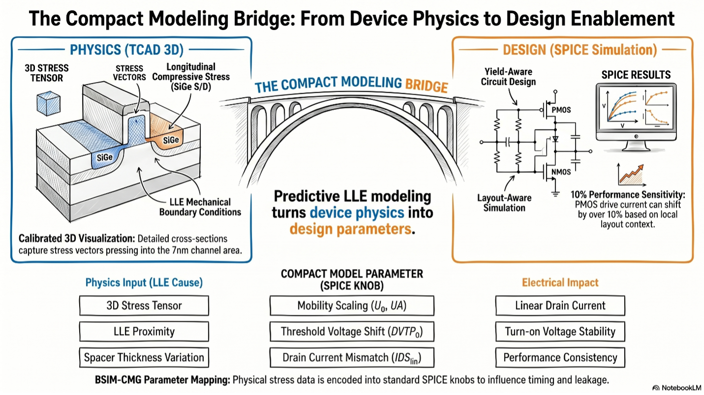
No matter how good a TCAD model is, it does not influence design unless its conclusions can be translated into a form that circuit and library teams can use. That is why one of the most important steps in the work is the mapping of layout-sensitive behavior into BSIM-CMG-relevant compact-model parameters, including U0, UA, DVTP0, DVTP1, DVTP2, and LPE0. This is the point where stress physics becomes directly useful to SPICE simulation.
That translation matters because many layout-dependent effects show up first as shifts in mobility, threshold voltage, or effective short-channel behavior. If those shifts remain trapped inside a device-level explanation, they are informative but not actionable. Once they are encoded into compact-model-relevant parameters, however, they can influence circuit-level timing, leakage, sensitivity analysis, and library characterization. In other words, this mapping is what allows layout-dependent stress to enter the same design infrastructure that already handles voltage, temperature, and process corners.
This is especially important for PMOS-sensitive structures, where the observed variability can be well beyond what would be considered a negligible correction. When PMOS current moves by more than 10% in certain local conditions, the effect cannot be left outside the compact-model layer. If it is not captured there, it will reappear later as unexplained mismatch between silicon behavior and circuit prediction.
3. What Do These Results Mean for PDK Development?
Once layout-sensitive behavior is representable in compact models, the natural next step is to ask how much of that knowledge should be reflected in the PDK. This is where the work becomes especially relevant to practical technology enablement. A modern PDK is not just a collection of nominal devices and design rules; it is also a way of encoding what the technology team believes designers need to know in order to use the process safely and efficiently. Stress-related LLEs clearly belong in that conversation.
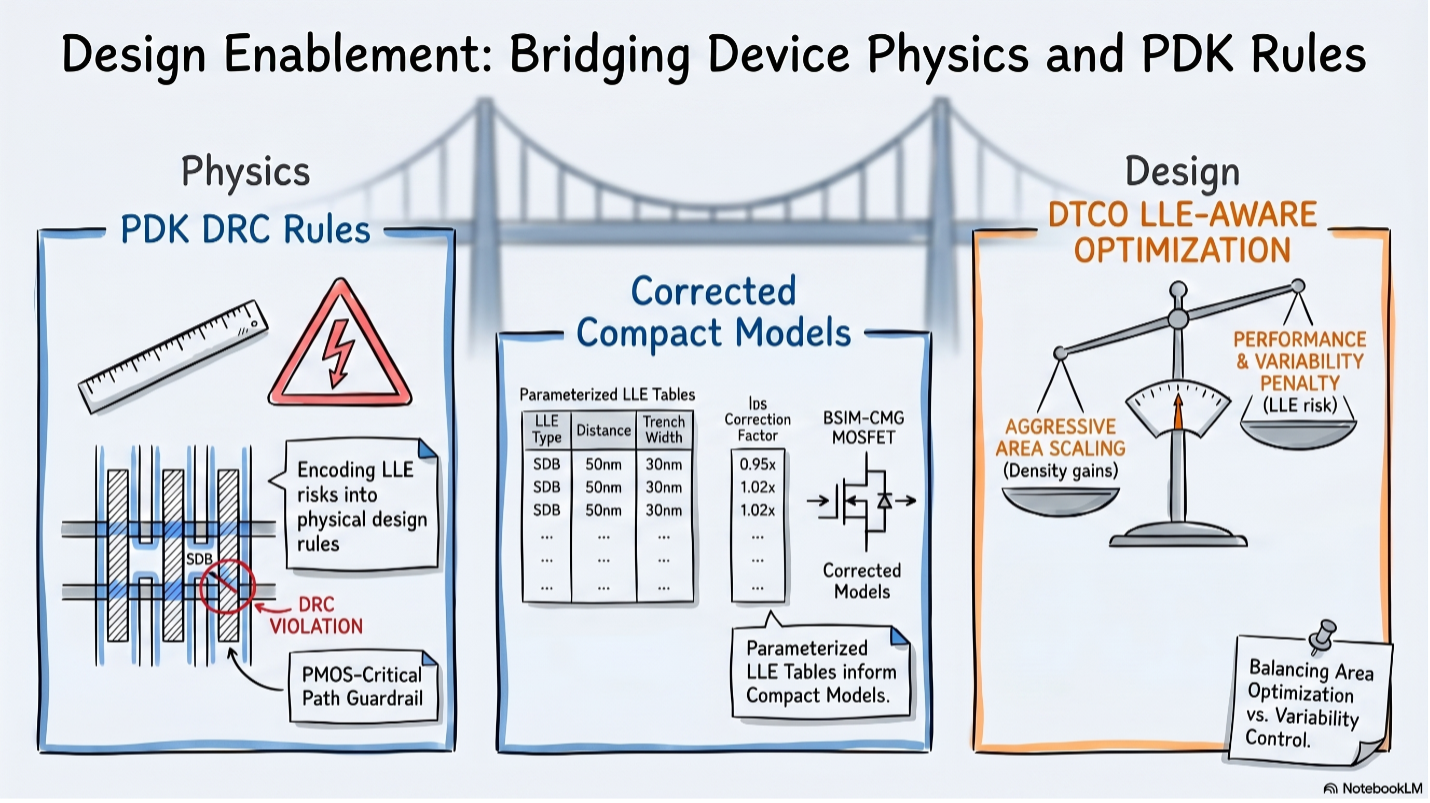
There are several obvious ways in which the results can inform PDK development. Layout-sensitive variability can be reflected through LLE tables, parameterized correction terms, stress-aware design-rule checks, or context-dependent model options for structures known to be vulnerable. In PMOS-critical regions, for example, proximity to diffusion breaks or aggressive gate-cut conditions may deserve explicit treatment rather than being left as an undocumented sensitivity. The same applies to integration-sensitive knobs such as trench width and spacer thickness when they are known to have a strong PMOS impact.
This is not about overcomplicating the PDK with excessive detail. It is about making sure the most important and most repeatable sensitivities are visible early enough to help design teams avoid pathological cases. A PDK that ignores the strongest stress-related LLEs may still be nominally functional, but it will force more risk and more variability management onto downstream design teams.
4. Why Does DTCO Need LLE Awareness, Not Just Density Awareness?
One of the clearest broader lessons from the work is that DTCO cannot be treated purely as an area-and-routability exercise. Modern density gains increasingly come from architectural compaction, layout restructuring, reduced cell height, tighter diffusion spacing, and more aggressive design-rule assumptions. But the results across the study show that these same choices can also intensify the coupling between active devices and their local mechanical environment. That creates a direct trade-off between density optimization and variability control.
This is exactly where LLE-aware modeling becomes useful to DTCO. Instead of evaluating a new cell architecture or layout style only in terms of area and nominal performance, the framework makes it possible to ask whether that same architecture also introduces a stronger stress penalty, a worse PMOS sensitivity, or a tighter process window. That kind of information is critical, because the cost of a density gain can be hidden until much later if variability is not assessed alongside it.
The work therefore supports a broader view of DTCO: not just power, performance, and area, but power, performance, area, and variability. At advanced nodes, those objectives are too strongly coupled to be treated independently. If a layout trick improves area but amplifies stress-related uncertainty, then it is not really “free” scaling.
5. How Does the Framework Help Process Optimization?
The design side is only half the story. The same framework is also useful on the process-optimization side because it identifies which integration knobs are strong, which are weak, and which matter mainly for PMOS. That is valuable because process optimization at advanced nodes is always a prioritization problem: many parameters can be adjusted, but not all of them deserve the same attention. The results make that prioritization much clearer.
Some examples stand out. Gate Cut timing shows meaningful stress sensitivity and therefore deserves process-aware treatment. Dielectric isolation choice emerges as a major PMOS lever, with performance changes ranging from strong improvement to strong degradation depending on material selection. SDB trench width produces a narrow process window because over-etching can sharply penalize PMOS. Spacer thickness is another PMOS-critical knob, even when the geometric deviation is only a few angstroms. By contrast, spacer deposition method produces a much smaller electrical impact and can therefore be treated with lower priority from an LLE standpoint.
That ranking is extremely useful. It helps technology teams focus control effort, metrology attention, and DTCO analysis where it matters most. Instead of treating every integration detail as equally dangerous, the framework identifies where the true stress-sensitive bottlenecks lie.
6. How Does This Lead to Better Guidance Earlier in the Flow?
One of the recurring themes in this series is that the earlier a sensitivity is understood, the cheaper it is to manage. The work supports exactly that kind of early guidance. Once a given layout feature or process knob is known to perturb PMOS stress strongly, there is an opportunity to translate that knowledge into design guidance, layout recommendations, or technology guardrails before it turns into a product-level issue.
That can take several forms. A design team may be advised to avoid certain gate-cut strategies in PMOS-critical regions. A layout rule may discourage aggressive diffusion-break proximity under specific device conditions. A technology team may tighten control on trench width or spacer thickness because the PMOS penalty is known to be too large otherwise. The exact implementation can vary, but the broader value is the same: the framework provides a path from physical understanding to earlier and more actionable engineering decisions.
This is particularly important in industrial settings where time-to-market matters. Variability that is understood only after silicon arrives is expensive. Variability that is represented in compact models, PDK assumptions, and layout guidance can often be avoided or at least bounded much earlier.
7. What Are the Real Limits of the Current Framework, and Why Do They Matter?
A credible engineering framework has to be explicit about its scope. One of the strengths of this work is that it does not claim to solve every variability problem at once. The analysis focuses on localized process variability, layout-dependent stress modulation, and the associated electrical impact. It does not attempt to reproduce full wafer-scale variability or all possible manufacturing fluctuations across the entire fab environment.
There are several practical limitations that matter. Some process assumptions remain constrained by the proprietary nature of the underlying technology. The framework is strongly grounded in one advanced 7nm FinFET context, which means direct transfer to another node or foundry would require requalification. There are also inevitable limits related to measurement noise, computational cost, static geometry assumptions, and the simplifications needed to make the stress and process model computationally tractable.
These are not weaknesses in the negative sense. They are what make the framework realistic. A model that tries to include every possible source of variability often becomes too broad to be useful. By focusing on the stress-related LLE problem with well-defined scope, the framework becomes much more actionable. The important point is not that it captures everything, but that it captures the right things well enough to inform design and technology decisions.
8. Why Do AI and ML Naturally Enter the Picture?
As the work expanded from measurement into modeling and process exploration, one future direction became especially clear: the next bottleneck is not only physical understanding, but throughput. A calibrated TCAD framework can be very powerful, but it is not cheap to run across a large combinatorial space of layout contexts, process splits, and temperature conditions. This is exactly where AI and ML become attractive extensions.
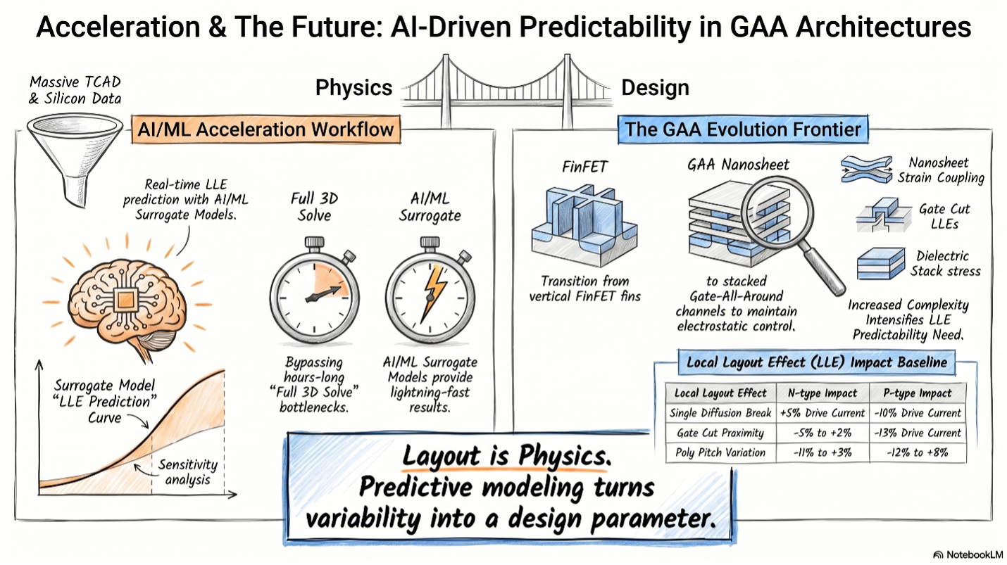
There are at least two obvious roles for AI/ML here. The first is surrogate modeling: learning compact predictors from a large body of TCAD and silicon data so that layout-sensitive stress behavior can be estimated much faster than with full simulation. The second is DOE optimization: using data-driven strategies to decide which layout or process cases are most informative to measure or simulate next, rather than exploring the space manually. Both directions would make LLE-aware development more scalable and more practical in a real industrial setting.
This is one of the most promising future extensions because it preserves the physics foundation while improving deployment efficiency. The goal would not be to replace physical modeling, but to accelerate and generalize it. In that sense, AI/ML would act as a force multiplier for a framework that is already physically grounded.
9. What Is the Next Frontier: Compound LLEs?
Another important limitation of the current framework is also a natural research direction: many real layouts contain multiple LLE mechanisms at once. In the current flow, much of the analysis is built around carefully isolated effects—Diffusion Breaks, Gate Cuts, poly pitch, fin pitch, and specific process knobs—because isolation is the right way to establish causality. But real product layouts often combine several of these perturbations simultaneously.
That leads naturally to the next frontier: compound LLE modeling. Instead of asking how one feature perturbs the channel, the problem becomes how several nearby features interact, whether their effects add linearly, compete, or create new boundary conditions that are not obvious from isolated studies. This is likely to become even more important as standard-cell architectures, track heights, and local routing environments continue to compress.
The current work provides a foundation for that future step because it already isolates the main first-order contributors and translates them into physically interpretable stress channels. That is exactly what is needed before more complex layout contexts can be treated with confidence.
10. Beyond FinFET: Why Won’t GAA Make the Problem Disappear?
A natural question is whether moving from FinFET to Gate-All-Around (GAA) architectures will reduce the importance of stress-related LLEs. The short answer is: not really. The underlying mechanisms may evolve, but the broader problem remains. GAA architectures change the electrostatic and geometric landscape, but they do not eliminate the fact that the channel sits inside a highly integrated mechanical environment shaped by local geometry, materials, and process sequence.
In fact, the work points in the opposite direction: the same need for layout-aware, stress-aware, and predictive modeling is likely to remain highly relevant as architectures evolve. If anything, more complex 3D structures and tighter integration may increase the need for frameworks that can connect geometry, process, and electrical response. That is why extension to GAA technologies is such a natural future direction.
This is also where the broader engineering message of the series becomes most durable. The exact device architecture may change, but the principle does not: local context matters, and advanced scaling increasingly depends on understanding how that context interacts with materials and process physics.
11. What Is the Broader Engineering Lesson?
The deeper lesson behind all of this is that stress-related LLEs sit at the intersection of several engineering layers that are too often treated separately: device physics, process integration, compact modeling, PDK development, and DTCO. The work becomes valuable precisely because it does not stop at any one of those layers. It starts from silicon, explains the physics with TCAD, connects the results to compact models, and points toward practical design and process implications.
That is also why this topic feels more important than a narrow variability study. It is not only about one set of PMOS current shifts or one class of layout features. It is about the fact that advanced-node development now depends on understanding interactions that used to be small enough to ignore. In that sense, stress-related LLEs are not an exception to scaling—they are one of the clearest examples of what scaling has become.
Once that is clear, the role of predictive modeling becomes obvious. It is not an academic add-on; it is part of how modern technology is made usable.
Conclusion
The practical value of stress-related LLE analysis lies in what it enables beyond device characterization. By combining large-scale silicon data, layout-aware DOE, calibrated 3D TCAD, and compact-model mapping, the framework creates a path from local mechanical sensitivity to SPICE-level predictability, PDK guidance, DTCO decisions, and process optimization. That is what turns a difficult device-physics problem into something that can actually improve how advanced technology is developed and used.
At the same time, the work has clear and realistic boundaries. It focuses on localized stress-related variability, not full manufacturing variation, and it remains tied to the assumptions of a specific advanced FinFET context. But that focus is exactly what gives it strength: it solves a hard and relevant problem well enough to matter.
The future directions are equally clear. AI/ML-assisted modeling, compound LLE analysis, and extension to GAA architectures are all natural next steps. And all of them build on the same central idea that has run through the entire series: at advanced nodes, layout is no longer just geometry. It is part of the device physics, part of the process problem, and part of the design problem too.

Final Note
This series started from a simple question: why two nominally identical transistors can behave differently depending on their local neighborhood? But it ended with a broader one: how semiconductor development changes once local context becomes a first-order physical variable? That shift is what makes stress-related LLEs so interesting. They reveal how deeply layout, process integration, and modeling are now coupled in advanced CMOS.
And that, more than any single result, is the real takeaway: the future of scaling depends not only on making devices smaller, but on making their interactions more predictable.