
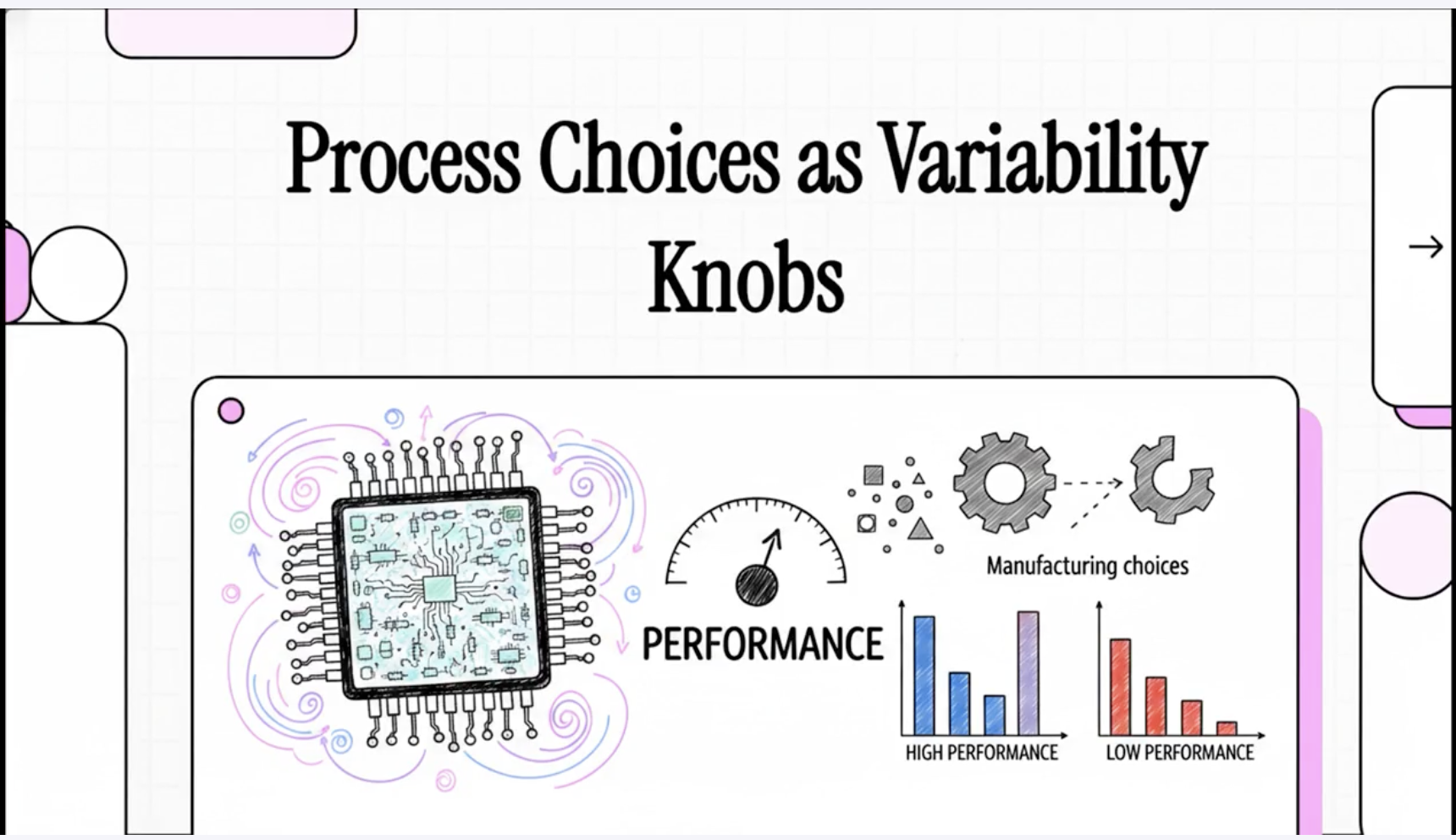
The previous post focused on the strongest layout-sensitive mechanisms observed on silicon: Diffusion Breaks and Gate Cuts, and the way they perturb local stress strongly enough to change transistor behavior, especially in p-type FinFETs. But once those mechanisms are understood, a more practical question immediately follows: what makes them better or worse? In other words, which parts of the process flow amplify stress-related Local Layout Effects, and which ones reduce them?
That is where process integration becomes just as important as layout. At advanced nodes, variability is not driven only by nominal device geometry. It is also shaped by the details of how materials are deposited, how isolation is formed, how aggressively trenches are etched, how thick spacers end up after fabrication, and even at what temperature the device operates. Those choices can alter the local mechanical environment enough to shift electrical behavior in a measurable way.
What makes this especially important is that these are not abstract simulator knobs. They are real integration parameters with direct consequences for performance, variability, process window, PDK assumptions, and DTCO trade-offs. Some of them produce only minor electrical shifts. Others change PMOS behavior dramatically. And because the underlying mechanism is stress-driven, the same process choice can affect PMOS and NMOS very differently.
This post focuses on those process-sensitive levers: how Gate Cut timing, dielectric materials, SDB trench width, spacer thickness, and temperature reshape the local stress state and, with it, the electrical response of the device.
1. How Does Layout Sensitivity Translate into Process Sensitivity?
A useful way to think about stress-related LLEs is that layout defines the mechanical boundary conditions, while process integration determines how strongly those boundary conditions are translated into actual stress in the channel. The geometry may decide where the transistor is exposed to a perturbation, but the process flow decides how that perturbation is created, transmitted, or relaxed.
That means two layouts with the same nominal intent may not behave the same way if the surrounding process assumptions change. A slightly different dielectric, a different gate-cut sequence, a change in trench etch, or a small thickness drift in the spacer can all modify the local stress environment enough to change the magnitude of the LLE response. In practice, this turns several integration details into variability knobs, parameters that may not define the transistor electrically in the classical sense, but still have a measurable impact on its final behavior.
This is one of the reasons why advanced-node variability cannot be treated only as a device-design problem or only as a layout problem. It sits at the interface between layout, materials, process sequence, and stress physics. The process studies make that very clear.
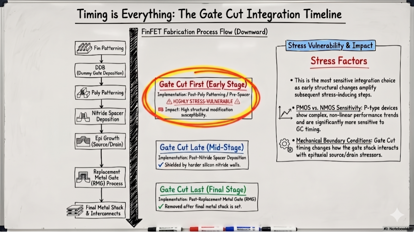
2. How Does Gate Cut Timing Alter the Mechanical Outcome?
One of the clearest examples of process-dependent stress modulation comes from Gate Cut timing. The position of a gate cut already matters as a layout feature, but the process sequence used to implement it matters as well. Different integration timings, such as GC First, GC Late, and GC Last, do not leave the device in the same mechanical state, even if the nominal geometric outcome looks similar.
The results show that Gate Cut timing has a strong impact on stress sensitivity, with GC First emerging as the most sensitive option. This is an important result because it means that the final LLE behavior is shaped not only by where the cut is located, but by when the cut is introduced during integration. The local stress field depends on the processing history, not just the final mask geometry.
From a practical point of view, this has direct implications for DTCO and process development. If a gate-cut strategy is chosen only for patterning convenience or integration compatibility without considering its effect on local stress, part of the penalty may appear later as PMOS variability or reduced performance margin. This is exactly the kind of trade-off that becomes visible only when layout sensitivity and process integration are analyzed together.
3. What Is the Impact of the Gate Spacer Deposition Method?
Not every integration knob produces a dramatic shift. One useful counterexample is gate nitride spacer deposition. Different deposition approaches, such as LPCVD, PECVD, and ICPCVD, were evaluated to understand whether the mechanical properties of the spacer film significantly change the electrical response through stress modulation.
The result is interesting precisely because it is relatively modest: the impact of spacer deposition method remains small, with performance variation of at most about 0.65% for n-type devices and 2.3% for p-type devices. In other words, this is not one of the dominant stress knobs in the same way that gate-cut timing or dielectric isolation can be.
That does not mean it is irrelevant. Even a small variation can matter when margins are tight, and the result still provides a useful ranking of sensitivity. It shows that some process choices affect stress-related LLEs only weakly, while others deserve much more attention. Knowing which is which is itself valuable for process optimization, because it helps focus effort where the payoff is real.
4. Why Is Dielectric Isolation One of the Strongest Process Knobs?
Among all the process knobs studied, dielectric isolation material stands out as one of the most influential. The local dielectric environment affects the stress field through its mechanical properties, such as thermal expansion and elastic response, and therefore changes how strain is transferred to the active region. Multiple dielectric options were evaluated, including SiO₂ as a reference, several forms of Si₃N₄, as well as SiCOH, HfO₂, and ZrO₂-based alternatives.
The contrast between NMOS and PMOS is striking. For n-type devices, the sensitivity is moderate, with the maximum degradation on the order of 10% relative to the SiO₂ reference. But for p-type devices, dielectric choice becomes a major performance lever: depending on the material, the response ranges from roughly +23% improvement to about −21% degradation. Optimized or doped Si₃N₄-based stacks improve PMOS behavior, while some high-k or low-k alternatives can penalize it significantly.
This is a very important result because it shows how strongly PMOS stress sensitivity can be engineered, or damaged, through material selection. Dielectric isolation is not only a question of capacitance, leakage, or integration compatibility. At advanced nodes, it is also a mechanical design choice with a direct electrical consequence. For PMOS in particular, the dielectric environment can effectively amplify or suppress one of the most important mobility-related stress channels in the device.
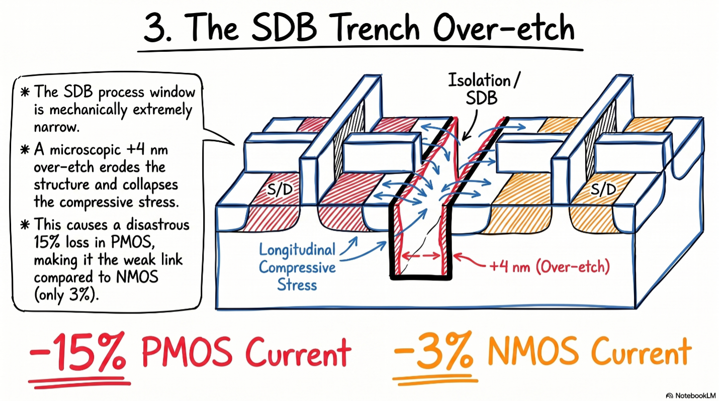
5. What Are the Real Consequences of SDB Trench Width Variations?
Another process knob with strong consequences is the Single Diffusion Break (SDB) trench width. This parameter may look like a manufacturing detail, but it directly affects the local geometry of isolation and therefore the stress field around the transistor. Small deviations in trench width—especially due to over-etching—can change the electrical response in a measurable and highly asymmetric way between device types.
The numbers make the point clearly. An over-etch of about +4 nm can degrade PMOS drive current by roughly 15%, while the NMOS penalty is much smaller, around 3%. The reason is again stress-related: PMOS performance depends strongly on the beneficial longitudinal stress established around the channel, and trench-width changes can erode that condition significantly. NMOS is affected as well, but less dramatically.
This result has a very practical interpretation: the SDB process window is mechanically narrow. Widening the trench may improve isolation from one perspective, but it can also destroy part of the beneficial PMOS stress state. Narrowing it may help preserve stress, but could introduce other concerns related to isolation, leakage, or reliability. This is a textbook example of how process integration becomes a multi-objective optimization problem at advanced nodes.
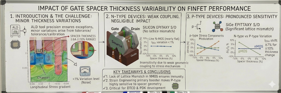
6. How Does Gate Spacer Thickness Variation Impact PMOS Devices?
If spacer deposition method had only a mild effect, spacer thickness variation turns out to be much more important. The analysis looks at roughly ±10% thickness changes, corresponding to only a few angstroms of geometric deviation, and asks a simple question: how much does that matter electrically?
For NMOS, the answer is: not very much. The electrical impact remains below about 1%, which makes spacer-thickness variability a relatively weak concern on the n-type side. For PMOS, however, the story is very different. A ±10% spacer-thickness variation leads to roughly ±7% shifts in linear-region current. That is a large effect for what appears, at first glance, to be a tiny geometric fluctuation.
This result is a strong reminder that PMOS stress sensitivity is not driven only by large visible layout features like gate cuts and diffusion breaks. It can also be modulated by much smaller process variations, especially when those variations influence the way the local stress field couples into the conduction path. In practical terms, this means that ALD uniformity, thickness control, and process metrology become much more important for PMOS predictability than a simplistic geometry-only view would suggest.
7. How Does Operating Temperature Influence Stress Sensitivity?
One of the most interesting results in the process studies is the effect of temperature. Layout sensitivity is often discussed as if it were a fixed geometric property, but the electrical manifestation of stress-related LLEs also depends on operating conditions. As temperature rises, mobility behavior changes, leakage increases, and the relationship between stress and current becomes weaker.
The quantified effect is substantial. When the temperature increases from 300 K to 375 K, the magnitude of LLE sensitivity decreases by about 80% for n-type devices and about 40% for p-type devices. In other words, the same local stress perturbation produces a much smaller electrical signature at elevated temperature.
This is important for two reasons. First, it confirms that the observed LLEs are strongly tied to mobility-stress coupling, because weakening that coupling with temperature also weakens the apparent electrical sensitivity. Second, it shows that variability is not a single-number property. The same device may show very different layout sensitivity depending on the thermal operating point, which has implications for timing analysis, corner definition, and reliability-aware design.
8. Why Does PMOS Consistently Emerge as the Most Critical Device?
Taken together, the process studies make one message very clear: PMOS is the critical device when it comes to stress-related variability knobs. Whether the perturbation comes from dielectric choice, trench width, or spacer thickness, the strongest electrical penalties consistently appear on the p-type side. That is fully consistent with the earlier layout studies, where PMOS already showed the strongest response to diffusion breaks and gate cuts.
This is not just a repetition of the same observation. It becomes more significant here because it shows that PMOS sensitivity is robust across both layout variables and process variables. The stress channels that matter most for hole transport remain exposed not only to local geometric changes, but also to multiple integration details. That makes PMOS a natural focal point for both characterization and mitigation.
In practical terms, this suggests a clear prioritization strategy: if variability-aware process optimization has limited bandwidth, PMOS-critical stress paths are where attention is most likely to deliver meaningful benefit. The data support that conclusion consistently.
9. How Do These Sensitivity Studies Translate into DTCO Inputs?
One of the most valuable aspects of these process studies is that they do not stop at reporting which knob is strong or weak. They directly suggest where DTCO, PDK development, and process control need to become more LLE-aware. The results point to several concrete directions: layout rules around gate-cut usage, stress-aware selection of dielectric materials, tighter control of diffusion-break etch conditions, and more careful treatment of spacer thickness on PMOS-sensitive structures.
This is exactly the kind of information that DTCO needs. It is not enough to know that one geometry is denser or more routable than another. At advanced nodes, the mechanical consequences of those choices also have to be understood. The process studies show that a technology cannot be optimized for area and performance alone if the resulting stress environment undermines variability and predictability.
In that sense, these variability knobs are not just post-silicon curiosities. They are co-optimization inputs. They define where process integration, layout strategy, and modeling infrastructure have to align if advanced-node behavior is going to remain predictable.
10. What Is the Broader Lesson About Local Stress as a Process Outcome?
The strongest conceptual lesson from these studies is that local stress is not only a consequence of device architecture or layout topology. It is also a process outcome. The final stress state in the channel is shaped by the integration history: what materials were chosen, how they were deposited, how isolation was etched, how thick the spacer became, and under what thermal conditions the device eventually operates.
That means variability at advanced nodes has to be understood as a layered problem. Layout defines the neighborhood. Process integration defines how that neighborhood is mechanically realized. Device physics then turns that mechanical condition into an electrical response. The process studies bring that full chain into focus in a way that purely geometric sensitivity analysis cannot.
This is also why predictive modeling becomes so valuable. Once these process knobs are recognized as real stress levers, they can no longer be treated as isolated fab parameters. They have to be represented in a framework that connects integration choices to electrical impact. That is the only way they can meaningfully inform design and technology decisions.
Conclusion
The process studies show that stress-related Local Layout Effects are not controlled by layout alone. Gate Cut timing, dielectric isolation, SDB trench width, spacer thickness, and temperature all act as real variability knobs, capable of changing the local stress environment and, with it, the electrical response of the device. Some effects are modest, such as the limited sensitivity to spacer deposition method. Others are much stronger: PMOS can improve by about 23% or degrade by about 21% depending on dielectric choice, lose roughly 15% with SDB over-etch, or shift by about ±7% under realistic spacer-thickness variation. Temperature, meanwhile, strongly attenuates the apparent sensitivity, especially on the NMOS side.
Taken together, these results make a larger point. In advanced FinFET technologies, variability is shaped not only by what is drawn in the layout, but also by how the process flow mechanically realizes that layout. Process integration choices are therefore part of the stress problem, part of the variability problem, and ultimately part of the design problem as well.
That is why these knobs matter. They turn local stress from an abstract physical concept into something that can be optimized, controlled, and engineered—provided the technology flow treats variability as a coupled problem across layout, process, and modeling.
What Comes Next
In the next article, I will move from process knobs to the broader engineering picture: how these results can be translated into compact-model parameters, PDK guidance, DTCO rules, and eventually into a more predictive, variability-aware design methodology for advanced CMOS.