
The ideal product for pure-play foundries who are the foundation of the fabless supply chain
This product includes the following two modules: Manufacturing Analytics and Process Control.
Exensio Foundry provides pure-play foundries with a single point-of-truth for all of their manufacturing data and a powerful visualization environment to analyze their manufacturing operations.
Run with the Leader in FDC and Process Control
With support for all leading semiconductor equipment providers and over 24,000 semiconductor manufacturing machines worldwide managed within their respective foundries, Exensio Foundry is the industry leader in FDC and process control.
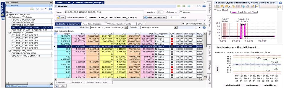
Managing and monitoring your factory floor has never been easier than with Exensio Foundry. The simple and intuitive interface enables engineers to select any machine sensor you want to control, set the upper and lower spec limits and view the raw data in the same dashboard. Full control of your fab has never been easier.
Find the Source of Critical Defects Quickly and Easily
DOWNLOAD 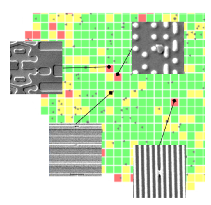 the Exensio Defect Management Data Sheet
Exensio® Defect Module enables manufacturers to load, preprocess, summarize and visualize data from multiple defect inspection steps. The Data Model designed and optimized for semiconductor manufacturing, aligns defect inspection data with all other data sources upstream and downstream including metrology, wafer sort, assembly and test data, final test and more. Powerful root-cause analysis tools enable users to fast and accurately identify defect sources and focus their efforts on things that matter.
Trusted by dozens of foundries, IDM’s, fabless and OSAT’s, Exensio® is the #1 commercial solution for end-to-end yield management in semiconductor manufacturing.
 Decades of experience in data integration
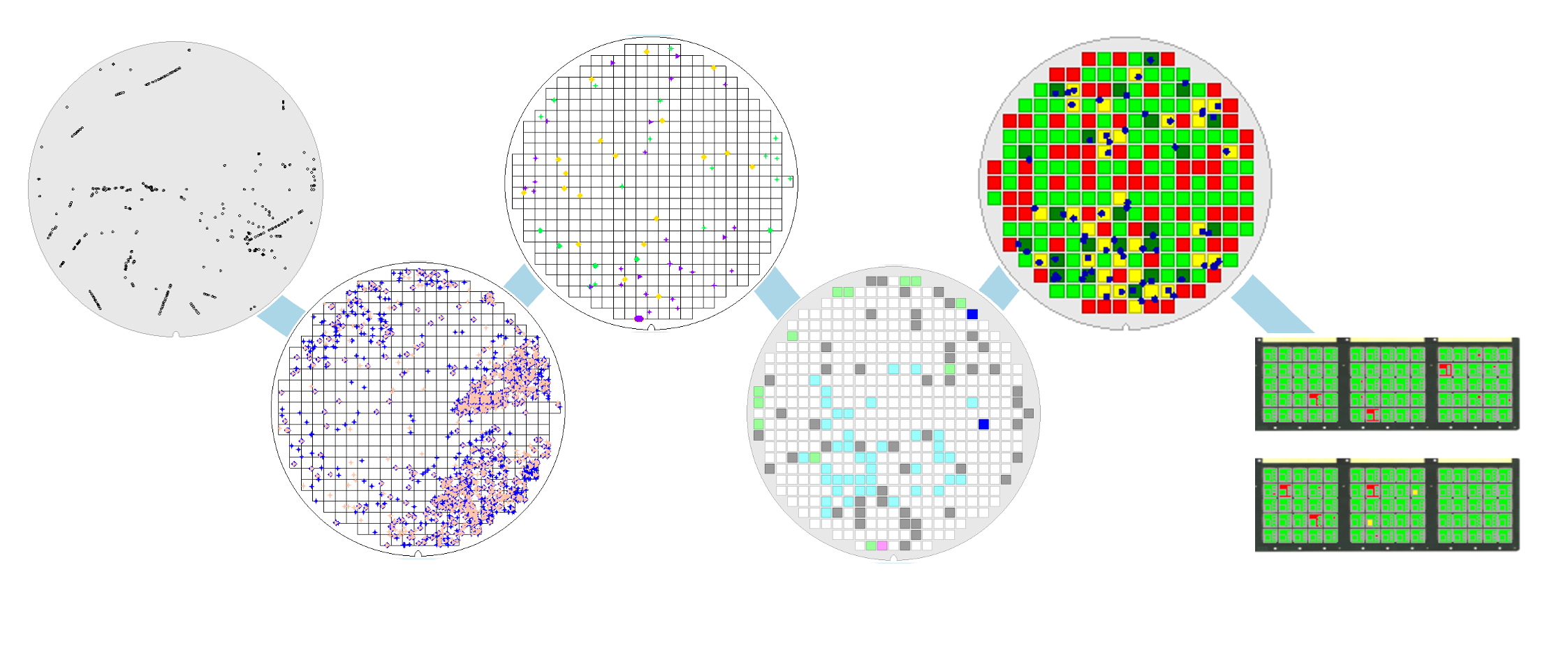
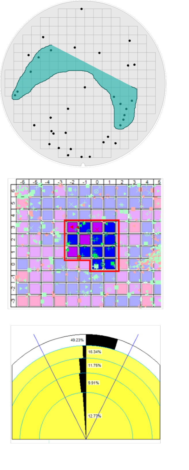
 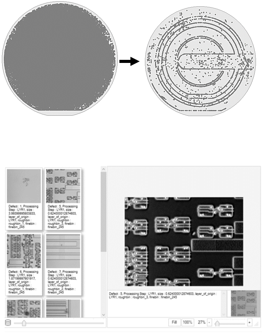 Sampling and Classification of Defects